Aluminum Nitride
Aluminum Nitride Substrates
Single crystalline aluminum nitride (AlN) is a promising material for a wide range of advanced applications in microelectronics and optoelectronics. Its outstanding properties include a wide band gap, high thermal conductivity and chemical stability. This makes it suitable for applications in optoelectronics (UV-C light emitting diodes (LED)s) for disinfection and metrology, power electronics ('High Electron Mobility Transistor` (HEMT) for electromobility, radio frequency technology for wireless communication (HEMT and 'surface acoustic wave` (SAW) filters) and high temperature sensing (thermocouples and piezoelectric elements) for temperature or force measurement in high temperature processes.
The high lattice matching of single crystalline AlN substrates to functional Al-rich AlGaN layers allows the fabrication of high quality AlN / AlGaN heterostructures, which are of central importance for the performance of the above devices in the diverse applications.
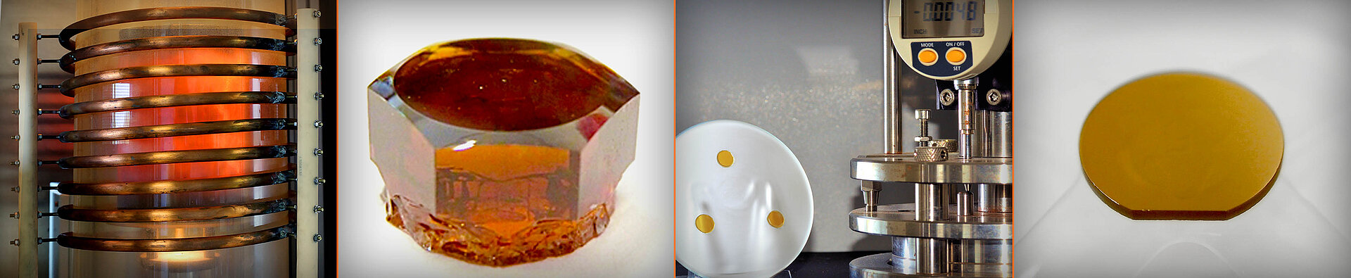
We have developed processes and technologies for the preparation of AlN substrates with low dislocation density, high UV transparency and high surface quality. Epi-ready single crystalline wafers are available from the IKZ in different quality grades according to the specification sheets for research purposes or for technology development.
Contact

Wide bandgap (6.2 eV)
High UV transparency at 265 nm and 230 nm
High thermal conductivity (170-230 W/mK)
Thermal expansion coefficient similar to Si
High chemical stability
High critical field strength
| Density | 3.2 |
| Bandgap Width [eV] | 6.2 |
| Thermal Conductivity [W/cmK] | 3.0 |
| Resistivity [Ohmcm] | >1013 |
| Dielectric Constant | 8.5 |
| Breakdown Field Strength [MV/cm] | 14 |
| Thermal Expansion Coefficient [1/K] | 4.5*106 |
IKZ offers semi-insulating Al-polar [0001] AlN substrates with 10 mm diameter and high crystalline quality - the typical dislocation density is 104 cm-2.
The substrates are optimized for the growth of AlN/AlGaN epitaxial layers for optoelectronic applications (UVC LEDs, LDs). Specifically, this means that the substrates are prepared with a tailored misorientation (<= 0.3°) for optimal AlGaN step growth and defect layers formed during mechanical processing are removed with a chemical-mechanical polishing process (Ra < 0.1 nm) developed at the IKZ.
If required, substrates with low absorption at low wavelengths and in particular at the wavelength of 265 nm used for disinfection applications can also be offered.
On request, the IKZ provides typical characterization data and advises on the requirement-specific selection of substrate properties.
- Optoelectronics
UV-C light emitting diodes (LED) for disinfection and metrology, as well as UV laser diodes (LD) - Power electronics
High Electron Mobility Transistor (HEMT) for electric mobility, - High frequency technology
High Electron Mobility Transistor (HEMT) and surface acoustic wave (SAW) filters for wireless communications - High temperature sensor technology
Thermo and piezo elements for temperature or force measurement in high temperature processes.
A. Dittmar, C. Hartmann, J. Wollweber, M. Bickermann:
(Sc, Y):AlN Einkristalle für Gitter-angepasste AlGaN Systeme;
DE102015116068A1