Technical Meeting Data
Date: Sep 7-9, 2016 (Wednesday noon through Friday noon)
Location:
![]()
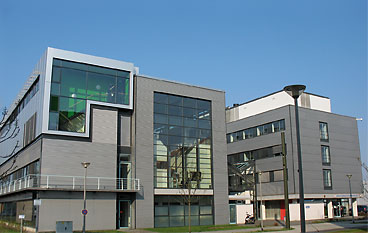
Leibniz Institute for Crystal Growth
seminar room 3.16 (capacity: 60)
Max-Born-Str. 2
12489 Berlin
Audience: Senior R&D staff from industry and academia
Invitation: International workshop “by invitation only”, send us an email if you’re interested to attend
Financial meeting data: No workshop fee. All travel, meals, and accomodation expenses are paid by the attendees themselves.
Co-organizers & Program Committee:
- Masataka Higashiwaki (NICT, Japan) (Chair)
- Matthias Bickermann (IKZ-Berlin, Germany) (Chair)
- Shizuo Fujita (Kyoto University, Japan)
- Yoshinao Kumagai (Tokyo University of Agriculture and Technology, Japan)
- Zbigniew Galazka (IKZ Berlin, Germany)
- Günter Wagner (IKZ Berlin, Germany)
- Oliver Bierwagen (Paul-Drude-Institut Berlin, Germany)
- Holger von Wenckstern (Universität Leipzig, Germany)
Meeting Contact:
Prof. Matthias Bickermann,
Leibniz Institute for Crystal Growth (IKZ), Max-Born-Str. 2, 12489 Berlin, Germany
Phone +49-30-6392-3047,
Fax +49-30-6392-3003,
Email:
matthias.bickermann@ikz-berlin.de
Program
- 17 invited lectures only, 30 mins. (plus 15 min. discussion) each:
- 6 on Wednesday, 7 on Thursday, 4 on Friday
- Poster session Wednes day afternoon
- Generous breaks between sessions for face-to-face discussions.
- > Program
List of Invited Speakers
- Prof. Shizuo Fujita (Kyoto Univ., Japan): Mist-CVD growth
- Dr. Michele Baldini (IKZ Berlin): MOCVD growth
- Prof. Takayoshi Oshima (Saga Univ., Japan): PLD and MBE growth
- Dr. Oliver Bierwagen (PDI Berlin): MBE growth
- Prof. Yoshinao Kumagai (TUAT, Japan): HVPE growth
- Akito Kuramata (Tamura Corp., Japan): EFG growth
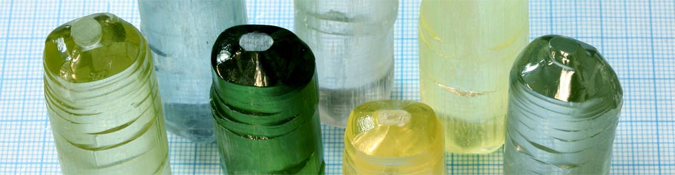
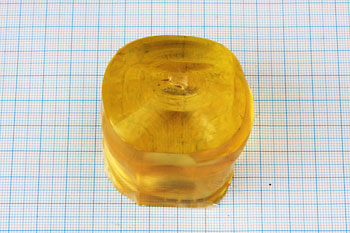
- Dr. Zbigniew Galazka (IKZ Berlin): Bulk crystal growth
- Dr. Chihiro Miyagawa (Fujikoshi Machinery Corp., Japan): Bulk crystal growth
- Dr. Martin Albrecht (IKZ Berlin): TEM investigations
- Prof. Takeyoshi Onuma (Kogakuin Univ., Japan): Optical characterization
- Dr. Klaus Irmscher (IKZ Berlin): Electrical and optical characterization
- Dr. Holger von Wenckstern (Univ. Leipzig, Germany): Photodetectors
- Prof. Masataka Higashiwaki (NICT, Japan): FET and SBD devices
- Dr. Gregg Jessen (AFRL, USA): Sn-doped LMOSFET devices
- Prof. Debdeep Jena (Cornell Univ., USA): Novel devices and device concepts
- Dr. Thomas Detzel (Infineon, Austria): Industrial aspects on power electronics materials
- Dr. Joachim Würfl (FBH Berlin): Prospects and challenges of power electronics
This event is generously supported by Berlin Partner for Business and Technology.
![]()
About the Meeting
Gallium oxide (Ga2O3) semiconductor electronics is emerging due to the material’s advantageous properties such as high band-gap and controllable doping from semi-insulating to conductive behavior. Ga2O3-based devices (field effect transistors, Schottky barrier diodes, photodetectors) with very promising properties have been demonstrated recently. However, the materials related technology is very challenging and there are a number of open issues in regard to a technology transfer to industry.
This meeting seeks to bring together leading scientists from industry and academia to discuss the challenges as well as the perspectives of Ga2O3-based electronics from a materials technology point of view, and to build up a dedicated community. The topics span from bulk crystal, substrate, and epilayer preparation to structuring, device technology, and characterization.
The meeting is held in Berlin, Germany, in the context of the recently founded Leibniz ScienceCampus “Growth and fundamentals of oxides for electronic applications“ (GraFOx), with a strong participation of Japanese scientists, who are the leaders in this field.
The meeting is hosted by the Leibniz Institute for Crystal Growth (IKZ) Berlin. During the meeting, the IKZ will offer a lab tour, and there are possibilities to visit to neighboring institutes (FBH, ISAS, Humboldt University, PDI) on request.