This event is generously supported by Berlin Partner for Business and Technology.
![]()
About the Meeting
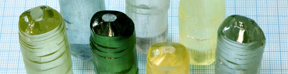
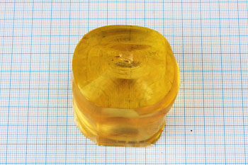
Gallium oxide (Ga2O3) semiconductor electronics is emerging due to the material’s advantageous properties such as high band-gap and controllable doping from semi-insulating to conductive behavior. Ga2O3-based devices (field effect transistors, Schottky barrier diodes, photodetectors) with very promising properties have been demonstrated recently. However, the materials related technology is very challenging and there are a number of open issues in regard to a technology transfer to industry.
This meeting seeks to bring together leading scientists from industry and academia to discuss the challenges as well as the perspectives of Ga2O3-based electronics from a materials technology point of view, and to build up a dedicated community. The topics span from bulk crystal, substrate, and epilayer preparation to structuring, device technology, and characterization.
The meeting is held in Berlin, Germany, in the context of the recently founded Leibniz ScienceCampus “Growth and fundamentals of oxides for electronic applications“ (GraFOx), with a strong participation of Japanese scientists, who are the leaders in this field.
The meeting is hosted by the Leibniz Institute for Crystal Growth (IKZ) Berlin. During the meeting, the IKZ will offer a lab tour, and there are possibilities to visit to neighboring institutes (FBH, ISAS, Humboldt University, PDI) on request.