Wednesday, Sept. 7 - 18:30
- Low-temperature growth of β-Ga2O3:Si (100) films on MgO (100) substrates
Ryo Wakabayashi1, K. Yoshimatsu1, and A. Ohtomo1,2
1 Department of Chemical Science and Engineering,
2 Materials Research Center for Element Strategy, Tokyo Institute of Technology, Japan - Photoelectron Satellites in Ga2O3 single crystals
Dieter Schmeißer and Jörg Haeberle
Angewandte Physik – Sensorik, Brandenburgische TU Cottbus, Konrad-Wachsmann-Allee 17, 03046 Cottbus, Germany - Czochralski Growth of β-Ga2O3 Crystals
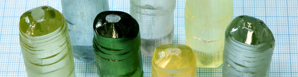
John Blevins1, Darren Thomson1, Kevin Stevens2, Greg Foundos2, and Wolfgang Schlichting2
1 Air Force Research Laboratory, Sensors Directorate (AFRL/RYDD), 2241 Avionics Circle, Wright-Patterson Air Force Base, Ohio 45433, USA;
2 Northrop Grumman Corporation, Aerospace Systems, SYNOPTICS, 1201 Continental Blvd., Charlotte, North Carolina 28273, USA - Temperature and stress distribution during growth of ß-Ga2O3 single crystals by the Czochralski method: numerical calculations
Klaus Böttcher1, Z. Galazka1, W. Miller1, and J. Schreuer2
1 Leibniz Institute for Crystal Growth (IKZ), Berlin;
2 Institute for Geology, Mineralogy and Geophysics, Ruhr University Bochum - Influence of incoherent twin boundaries on the electrical properties of homoepitaxial ß-Ga2O3 layers grown by metal organic vapor phase epitaxy
Andreas Fiedler, R. Schewski, M. Albrecht, M. Baldini, Z. Galazka, G. Wagner and K. Irmscher
Leibniz Institute for Crystal Growth, Max-Born-Str. 2, 12489 Berlin, Germany - Physical and Electrical Characterization Assessment of ß-Ga2O3 Capacitors with an Al2O3 Gate Dielectric
Chadwin D. Young Materials Science and Engineering and Electrical Engineering, University of Texas at Dallas, 800 W. Campbell Rd., RL10, Richardson, TX 75080, USA - ITO ohmic contacts for β-Ga2O3
Takayoshi Oshima1, Ryo Wakabayashi2, Mai Hattori2, Akihiro Hashiguchi1, Naoto Kawano1, Kohei Sasaki3,4, Takekazu Masui3,4, Akito Kuramata3,4, Shigenobu Yamakoshi3,4, Kohei Yoshimatsu2, Akira Ohtomo2, Toshiyuki Oishi1, and Makoto Kasu1
1 Department of Electrical and Electronic Engineering, Saga University, Japan;
2 Department of Chemical Science and Engineering, Tokyo Institute of Technology, Japan;
3 Tamura Corporation, Japan;
4 Novel Crystal Technology, Inc., Japan