Section Thin Oxide Films
Section Thin Oxide Films
Mission
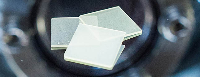
Oxide layers can be used as the electrically active part of a device offering new application prospects compared to bulk crystals and ceramics. By utilizing dopants or lattice strain, their functional properties can be specifically adapted to desired requirements. Smaller device structures in epitaxial thin layers not only provide less material consumption, but also allow improved device parameters such as higher processor speed or higher operation frequencies for filters or sensors. In addition, using remote epitaxy or sacrificial layers, free-standing oxide films and novel oxide heterostructures can be fabricated, which are not possible by conventional methods due to incompatibility of growth conditions, e.g. different lattice parameters or symmetries. Our mission is to develop single-crystal oxide films with optimized properties tailored to the application.
Research activities
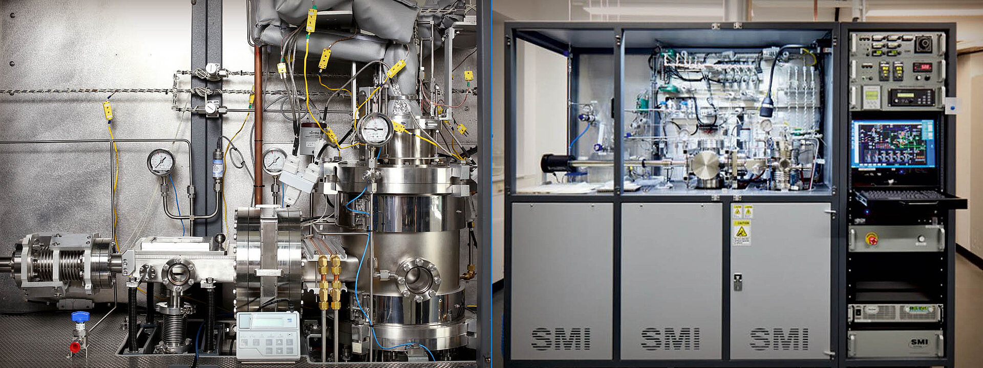
The main focus of our work is the development of oxide thin films with tailored semiconducting, dielectric or ferro/piezoelectric properties. The deposition methods available at IKZ are metal-organic vapor phase epitaxy (MOVPE) and pulsed laser deposition (PLD). Our activities include oxide films with thicknesses between a few nanometers and several micrometers with large potential for application in high-power electronics, ferroelectric memory devices, piezoelectric sensors and energy harvesters.
Head of Section

Topics
Epitaxy of semiconducting Gallium Oxide
Modern society relies on a wide range of electrical and electronic systems. To achieve this, the conversion of electrical energy must be carried out as efficient as possible. The material system β-Ga2O3 has due to its high bandgap of approx. 4.8 eV and the resulting theoretically high breakdown field strength the best prerequisites to become the high-performance material for next generation power applications. Therefore our mission is to achieve the predicted material properties through process development to pave β-Ga2O3 the way into power electronics.
The β-Ga2O3 MOVPE process development is focused on the investigation of the effects of the growth parameters and the type of doping on the electrical properties of the layers. Another focus is the homoepitaxial growth on differently oriented substrates and the influence on the generation of crystal defects. In addition, there are studies on increasing the growth rate by maintaining the good layer quality. In future, also alloys of the material with aluminium are planned to improve the positive properties of β-Ga2O3 even further.
S. Bin Anooz, R. Grüneberg, C. Wouters, R. Schewski, M. Albrecht, A. Fiedler, K. Irmscher, Z. Galazka, W. Miller, G. Wagner, J. Schwarzkopf and A. Popp
Step flow growth of β-Ga2O3 thin films on vicinal (100) β-Ga2O3 substrates grown by MOVPE
Appl. Phys. Lett.116, 182106 (2020)
DOI: 10.1063/5.0005403
T.-S. Chou, P. Seyidov, S. Bin Anooz, R. Grüneberg, J. Rehm, T.T.V. Tran, A. Fiedler, Z. Galazka, M. Albrecht, and A. Popp
High-mobility 4 μm MOVPE-grown (100) β-Ga2O3 film by parasitic particles suppression
Jpn. J. Appl. Phys. 62, SF1004 (2023). [Spotlight Article]
DOI: 10.35848/1347-4065/acb360
T.-S. Chou, P. Seyidov, S. Bin Anooz, R. Grüneberg, M. Pietsch, J. Rehm, T.T.V. Tran, K. Tetzner, Z. Galazka, M. Albrecht, K. Irmscher, A. Fiedler, and A. Popp
Suppression of particle formation by gas-phase pre-reactions in (100) MOVPE-grown β-Ga2O3 films for vertical device application
Appl. Phys. Lett. 122, 052102 (2023).
DOI: 10.1063/5.0133589
Contact

Strained functional perovskite films
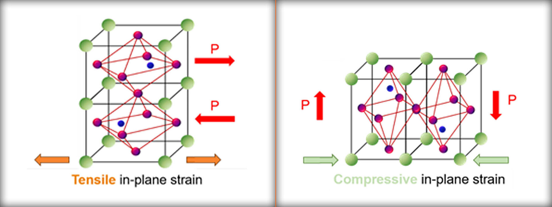
Functional oxide films with perovskite structure exhibit a variety of functional properties depending on their chemical composition and structure. In contrast to bulk crystals, in epitaxial layers additional degrees of freedom are given by incorporating lattice strain (strain engineering by heteroepitaxy) or intentional defects (defect engineering) to deliberately modify material properties and to develop new technologies. Our mission is to make promising materials with perovskite structure, such as the lead-free ferro/piezoelectric material Potassium-Sodium-Niobate ((K,Na)NbO3) or the dielectric Strontium-Titanate (SrTiO3), available in thin film form for potential applications, e.g. for highly sensitive sensors or neuromorphic computing.
In close collaboration with the sections "Oxides & Fluorides" and "Experimental Characterization", we grow (K,Na)NbO3 and SrTiO3 based films using the metal-organic vapor phase epitaxy (MOVPE) method as the only group worldwide. By introducing lattice strain or off-stoichiometry, material properties (such as piezoelectric constants, phase transition temperature, dielectric permittivity) are deliberately modified. In particular, film characterization using scanning probe microscopy techniques such as piezoelectric force microscopy (PFM) and conductive atomic force microscopy (CAFM), provides insight into ferroelectric domain formation and electrical properties at the nanometer scale.
Leonard von Helden, Laura Bogula, Pierre-Eymeric Janolin, Michael Hanke, Tobias Breuer, Martin Schmidbauer, Steffen Ganschow, and Jutta Schwarzkopf,
Huge impact of compressive strain on phase transition temperatures in epitaxial ferroelectric KxNa1-xNbO3 thin films
Appl. Phys. Lett. 114, 232905 (2019)
DOI: 10.1063/1.5094405
Dorothee Braun, Martin Schmidbauer, Michael Hanke and Jutta Schwarzkopf
Hierarchy and scaling behavior of multi-rank domain patterns in ferroelectric K0.9Na0.1NbO3 strained films
Nanotechnology 29, 015701 (2018)
DOI: 10.1088/1361-6528/aa98a4
Jutta Schwarzkopf, Dorothee Braun, Michael Hanke, Reinhard Uecker and Martin Schmidbauer
Strain engineering of ferroelectric domains in KxNa1-xNbO3 epitaxial layers
Front. Mater. 4, 26 (2017)
DOI: 10.3389/fmats.2017.00026
Contact
Sacrificial layers and free-standing oxide films
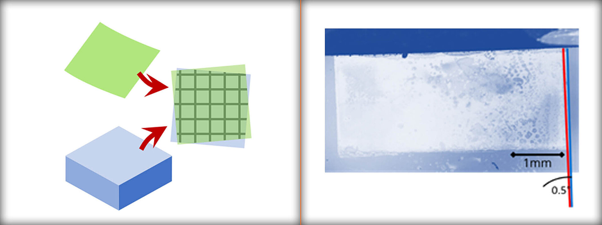
Alternatively, to strain engineering by heteroepitaxial film growth on lattice mismatched substrates, local lattice strain and strain gradients on the nanometer scale can be generated by the formation of artificial twist boundaries in oxide thin films. This is provided by the transfer of freestanding ultrathin oxide films on a single-crystal or another epitaxial oxide film with a controlled twist angle. Our mission is to explore the impact of the generated dislocation network on the dielectric and ferroelectric properties of thin complex oxides.
Um freistehende nanometerdünne Oxidschichten zu erzeugen wird das Konzept der Opferschicht (Sacrificial Layer), hergestellt mit Hilfe der gepulsten Laserdepositionstechnik (PLD), und dem Überwachsen der funktionellen Oxidschicht durch PLD oder MOVPE angewandt. Der Schichttransfer erfolgt mit unserer neu entwickelten Layer-Transferstation, die unter Hochvakuumbedingungen arbeitet (siehe Abschnitt "Nanostrukturen"). Wir wenden Rastersondenverfahren an um grundlegende Erkenntnisse über die Domänenbildung nach dem anschließenden Bonden auf einem neuen Substrat oder nach dem Anlegen einer externen Spannung zu gewinnen.
Contact