Gallium Oxide
Gallium oxide substrates and epi-layers
Gallium oxide
Over the past decade, beta-gallium oxide (β-Ga2O3) has emerged as a promising material for next-generation power electronics. Due to its wide band-gap properties, ease of n-type doping corresponding to a widely tunable conductivity, and high breakdown strength, devices made from β-Ga2O3 are ideal for power conversion applications, RF technology / wireless communication, and space applications. In addition, the commercialization potential for β-Ga2O3 is expected to be more than competitive in the power semiconductor market as a result of the development of low-cost, high-quality substrates.
Specifications
Gallium oxide substrates
A key prerequisite for the development of technologies based on gallium oxide is the availability of high-quality single crystalline substrates.
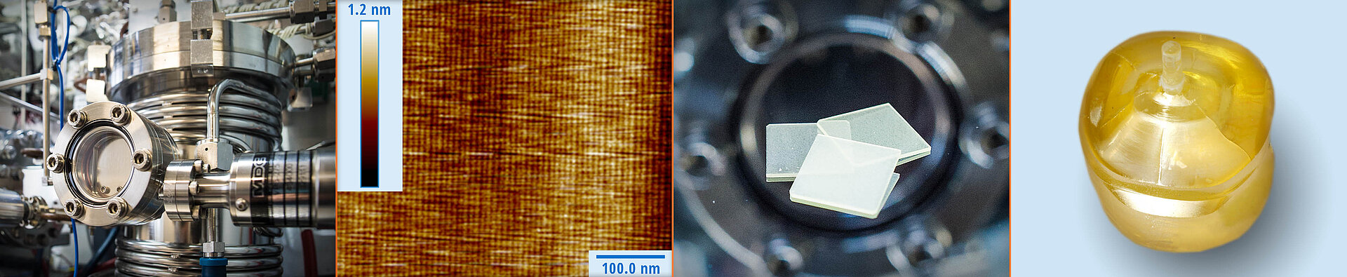
Here in IKZ, we have developed the growth of bulk gallium oxide (β-Ga2O3) single crystals of 2 inch in diameter by the Czochralski method using a proprietary technology. The crystals can be semi-insulating, semiconducting, and highly conducting (degenerate semiconductors). While conducting material is dedicated to research topics at IKZ, semi-insulating substrates (100), including offcut, can be obtained from our partner CrysTec GmbH.
Specifications
Gallium oxide epi-layers
In parallel to the bulk crystal growth,we made significant advancements in epitaxy technologies for growing device-level β-Ga2O3 layer with low defect density, high mobility, and high surface quality via MOVPE (Metal Organic Vapor Phase Epitaxy). The high-quality epi-layers are now available from IKZ with wide-range thickness and doping concentration as specified. Our epitaxy process is compatible with different β-Ga2O3 crystalline orientations (100) 4°off and (010) and has the potential for heteroepitaxy on foreign substrates, including Si, SiC, GaN… etc. Homo- and hetero-epitaxial layers can be customized with the specifications according to the datasheet.
Specifications
If you are interested in our service or have any specific requirements beyond those mentioned, please feel free to contact us directly.
Contact

- Wide bandgap (4.5-4.9 eV)
- High critical field strength (8 MV/cm)
- Low-cost native substrate availability
- High thermal stability
- Detector and Sensor
Visible-blind and solar-blind detectors, nuclear radiation detection, gas sensor (i.e., oxygen and hydrogen) - High-power radio frequency (RF) device
Radio-frequency amplifiers for wireless communications - High-power device
Power-switching for the electric grid, high voltage direct current (HVDC) transmission in electrical vehicles - Vertical device
Vertical diodes, field-plate Schottky diode, Trench-Schottky diode, MIS diode, vertical FinFETs - Lateral device
MESFET, MOSET, MODFETs (hosting a two-dimensional electron gas (2DEG))
Ta-Shun Chou, Saud Bin Anooz, Andreas Popp, Walter Haeckl:
Method for growing a gallium oxide layer on a substrate and semiconductor wafer;
EP22194558
T.-S. Chou, P. Seyidov, S. Bin Anooz, R. Grüneberg, J. Rehm, T. T. V. Tran, A. Fiedler, Z. Galazka, M. Albrecht, A. Popp,
High-mobility 4 μm MOVPE-grown (100) β-Ga2O3 film by parasitic particles suppression;
Jpn. J. Appl. Phys. 2023, 62, SF1004 | DOI:10.35848/1347-4065/acb360
T.-S. Chou, P. Seyidov, S. Bin Anooz, R. Grüneberg, M. Pietsch, J. Rehm, T. T. V. Tran, K. Tetzner, Z. Galazka, M. Albrecht, K. Irmscher, A. Fiedler, A. Popp,
Suppression of particle formation by gas- phase pre-reactions in (100) MOVPE-grown β- Ga2O3 films for vertical device application;
Appl. Phys. Lett. 2023, 122, 052102 | DOI: 10.1063/5.0133589
M. Lee, T.-S. Chou, S. Bin Anooz, Z. Galazka, A. Popp, R. L. Peterson,
Exploiting the Nanostructural Anisotropy of beta-Ga2O3 to Demonstrate Giant Improvement in Titanium/Gold Ohmic Contacts;
ACS Nano 2022, 16, 11988 | DOI:10.1021/acsnano.2c01957
Specifications
IKZ is growing gallium oxide bulk crystals via the Czochralski method and homo- and hetero-epitaxial layers by Metal Organic Vapor Phase Deposition (MOVPE).
Substrates: semi-insulating substrates can be acquired via our partner CrysTec GmbH [order here].
Epitaxial layers: IKZ offers homo- or heteroepitaxial gallium oxide layers with 5 × 5 or 10 × 10 mm2, low defect density, high electron mobility, and good surface quality. Detailed specifications can be found in the datasheet, and feel free to contact us if you have any questions or special requirements.
We are also open to joint research and development projects. If you have any questions or requests, please feel free to contact us.
General bulk properties
upITEM | SPECIFICATION |
| Density | 5.95 [g/cm³] |
| Bandgap Width | 4.5 - 4.8 [eV] |
| Thermal Conductivity | 0.1 - 0.3 [W/cmK] |
| Resistivity | Doping-dependent |
| Dielectric Constant | 10 |
| Breakdown Field Strength | 8 [MV/cm] |
Substrate properties
upITEM | SPECIFICATION | |
| Dopant | Mg (semi-insulating) | |
| Doping Level | - | |
| Orientation | (100)-Cz | |
| Misorientation | 4° | |
| Thickness | 0.5 mm | |
| Size | 5x5 mm2, 10x10 mm2 | |
Epi-layer properties
upITEM | SPECIFICATION | |
| Dopant | Si (n-type) | |
| Doping Level | 5x10¹⁶ - 2x1019 cm-3 | |
| Thickness | 4 nm - 4 μm | |