Joint Labs & Support Labs
Joint Labs & Support Labs
Labs
Joint Laboratory for Advanced Magneto-Transport Adlershof – JAMA
The joint Laboratory for Advanced Magneto-Transport is a facility of the Leibniz-Institut für Kristallzüchtung and the Humboldt-Universität zu Berlin. It combines the excellent equipment and complementary scientific expertise of both institutions to provide state-of-the-art high magnetic field and cryogenic infrastructure for solid state physics and materials science research and to make it available to both institutions and their partners with the aim of investigating modern electronic materials and compounds, in particular nano- and quantum structures in the field of electronics and photonics.
Research into transport phenomena and magneto-transport enables the determination of important material-specific parameters and the investigation of solid-state physical effects that are used in modern electronics. Conversely, the electrical measurements can also be used to draw conclusions about the quality of the material, such as the homogeneity of the structure.
At JAMA, three-, two-, one- and zero-dimensional structures made of new semiconductor materials, ultra-thin films, nanostructures and quantum systems are investigated. In addition, the surface and interface effects of spin, charge and heat transport in combinatorial material systems made of metals, semiconductors, superconductors and topological insulators are investigated. This leads to new hybrid structures, e.g. semiconductor/superconductor hybrids or metal/semiconductor hybrids, which can exhibit new physical phenomena. Physical phenomena in solids, which are investigated as a function of electric fields, weak and strong magnetic fields and temperature, include the determination of transport parameters (conductivity, charge carrier density), phase transitions, in particular to collective states (superconductivity, charge density waves), low-dimensional and topological electronic states. The influence of interfaces and surfaces and dimensionality is investigated in topological surface states, proximity effects, size effects of conductivity, magnetoresistance, thermoelectricity and thermal conductivity, and quantum phenomena.
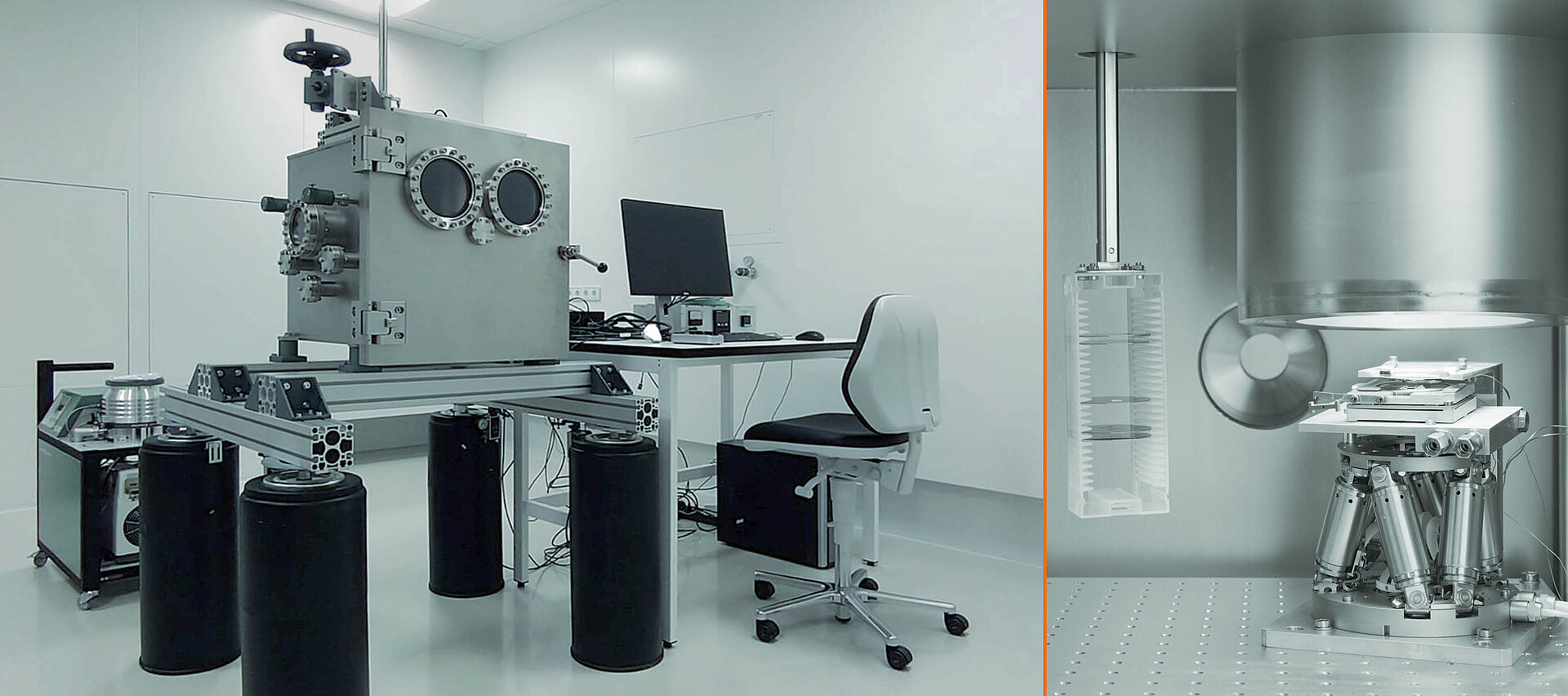
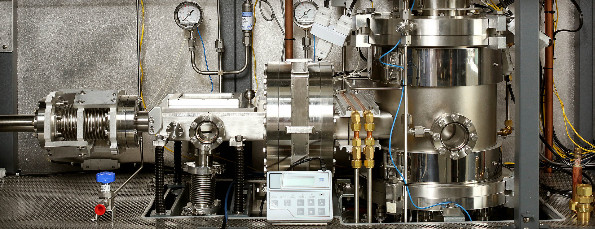
The JAMA enables the characterization of materials at low temperatures down to 25 mK and high magnetic fields up to 12 T. The low temperatures and high magnetic fields are achieved using a helium-3/helium-4 based Oxford Instruments Kelvinox JT insert in combination with an Oxford Instruments Teslatron PT closed-cycle refrigerator cryostat. The laboratory is equipped with state-of-the-art electrical measurement technology.
The JAMA meets a unique environment of university and non-university research institutions on the Adlershof campus and in Berlin and will strengthen the cooperation in research and teaching between the Humboldt-Universität zu Berlin and the Leibniz-Institut für Kristallzüchtung in the field of electronic high magnetic field and low-temperature transport phenomena.
Leibniz-Institut für Kristallzüchtung (IKZ):
Scientific coordination: Dr. Andreas Fiedler
Section: Experimental Characterization / Transport and Electrical Properties
Humboldt-Universität zu Berlin:
Scientific coordination: Prof. Dr. Saskia F. Fischer
AG Neue Materialien / Institut für Physik & Center of the Sciences of Materials Berlin
GNM Webseite (Deutsch): https://www.physik.hu-berlin.de/de/gnm/neue-materialien
GNM Webseite (Englisch): https://www.physik.hu-berlin.de/en/gnm-en/neue-materialien
Deutsch-Chinesisches Joint Lab (Dielektrika)
The German-Chinese Joint Lab between the School of Electronic Science and Engineering at Xi´an Jiaotong University and the Leibniz-Institut für Kristallzüchtung (IKZ) and was founded on the occasion of the international Workshop ´Oxide & Graphene` which took place from 14th to 15th January 2020. Our mission is to join forces on the long-term perspective of research and education in the area of dielectrics and 2D materials, covering fundamental as well as device physics.
Dielectric oxide layers and 2D materials with their plethora of functional properties are in the focus of worldwide research to understand their physical properties on the atomic – scale and to engineer their functional characteristics for future device applications. However, the complexity of these materials systems in terms of synthesis, thin film deposition, characterization as well as device processing and integration steps often exceeds the capacities available at individual laboratories. Hence, IKZ and Jiaotong University in Xi´an decided to establish a joint lab and benefit from synergies in complementary research activities and student education. Online lectures, exchange of PhD students and international workshops will be undertaken to promote the common goals. Currently, research focuses on the development of lead-free ferro-/piezoelectric layers for green technology in application areas like sensing & energy harvesting e.g. for the future Internet of Things (IoT). Furthermore, the fundamental physics and processing steps of 2D materials are investigated with the perspective to engineer future functional 3D crystals through advanced layer-by-layer transfer processes.
Xi'an Jiaotong-Universität:
Head: Prof. Gang Niu
Prof. Gang Niu´s webpage: http://gr.xjtu.edu.cn/web/gangniu
International School on Dielectics: http://esteie.xjtu.edu.cn/
IKZ:
Head: Dr. Jutta Schwarzkopf
Section: Nano Structures & Layers / Thin Oxide Films
Dr. Jens Martin
Section: Nano Structures & Layers / Thin Oxide Films / Topic: „2D goes 3D” by Layer Transfer

Joint Lab for Electron Microscopy Adlershof (JEMA)
The joint lab for electron microscopy is a facility operated by the Leibniz-Institut für Kristallzüchtung and Humboldt-Universität zu Berlin which shares the excellent equipment of both institutions, to develop the most modern methods in electron microscopy and make them available for both institutions and their partners to study structure property relations in crystalline materials.
Electron microscopy is the most versatile technique to obtain correlated information on structural and physical properties of solids with high spatial resolution. Transmission electron microscopy and scanning transmission electron microscopy made tremendous methodological advances in the last years. Due to the possibility to realize abberation corrected lenses true atomic resolution can be obtained with a resolution to 0.05 nm and a precision in the pm range. Analytical methods now allow for atomic resolution chemical mapping and electron loss spectroscopy achieves energy resolution that competes with that achievable in synchrotrons. The development of fast cameras with single electron sensitivity and sample holders that allow to follow processes in situ under biasing, at high temperature and under ambient pressure.
JEMA joins latest equipment in structural and analytical electron microscopy. While IKZ provides an aberration corrected (S)TEM (FEI Titan 80-300) equipped with a fast CETA2 camera (up to 400 frames per second) and latest in-situ holders that allow for operation under biasing and heating (Protochips Fusion) and at various gas atmosphere up to atmospheric pressure and temperatures up to 1000°C, Humboldt-Universität provides its (S)TEM with energy dispersive spectroscopy and energy loss spectroscopy.
The Leibniz-Institut für Kristallzüchtung in addition to transmission electron microscopes provides two scanning electron microscopes among them a fully analytical Dual Beam microscope (FEI Nova 600) that allows for structuring samples by an ion beam, and preparing electron transparent lamella from selected areas of a sample and lifting them out for further analysis in the TEM. This microscope provides in addition energy dispersive and wavelength spectroscopy and electron backscatter diffraction. A second, latest generation SEM Thermo Fisher Apreo S with three in-lens detectors and a STEM detector is equipped with a He cooling stage and a Gatan Monarc CL system to study optical properties of semiconductors.
JEMA has been the first joint activity in the field of electron microscopy in Adlershof. A similar centre exists now between Helmholtz Zentrum Berlin und HU Berlin in the field of cryomicroscopy. Other joint labs are on the way, all of them offering complementary equipment, thus making the Campus Adlershof a true centre for electron microscopy in Berlin.
Read more: https://csmb.hu-berlin.de/beam/
Contact IKZ

IKZ-DESY Joint Lab
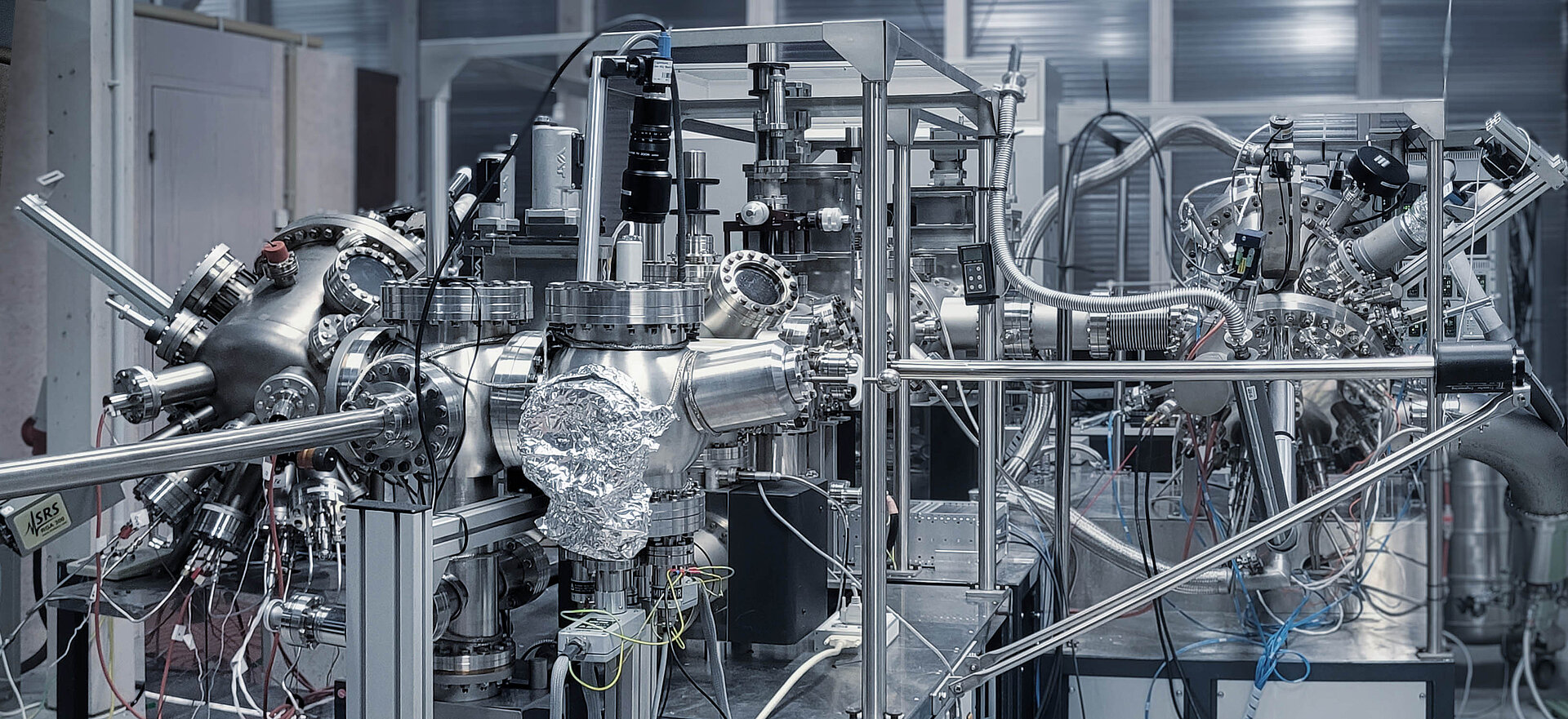
The IKZ-DESY Joint Lab between the Leibniz-Institut für Kristallzüchtung (IKZ) and the German Electron-Synchrotron (DESY) bundles and coordinates the activities of IKZ on the Science Campus Hamburg Bahrenfeld. Located in the Center for X-Ray Nanoscience (CXNS), it is an integral part of the cooperation between the two institutions. The Joint Lab supports the IKZ in-house research by offering access to advanced Synchrotron methods. In addition, crystalline materials from IKZ and advanced methods for research at synchrotrons are being developed to improve the performance of existing and future lightsources. As a third pillar the Joint Lab together with DESY Innovation Office aims to forward the transfer of original research toward the market, e.g., via foundation of StartUps.
The IKZ research group X-Ray Optics and DESY Nanolab operate a joint laserlab for time-resolved ultrafast spectroscopy at the IKZ-DESY Joint Lab. The setup is open for experimental characterization of IKZ materials and methods using various optical techniques. IN addition, the lab is used for preparation experiments for synchrotron beamtimes.

IKZ-Cornell Joint Lab for Unleashing Hidden Properties to Empower Oxide Electronics
The German-American Joint Lab between Cornell University and the Leibniz-Institut für Kristallzüchtung (IKZ) was launched with the 2020 appointment of Prof. Darrell G. Schlom as a Leibniz Chair at IKZ following two decades of fruitful collaboration with him and his group. Our joint mission is the coordinated research on the development of large-area single-crystal oxide substrates enabling the discovery of materials with unprecedented properties for the next generation of oxide electronic devices.
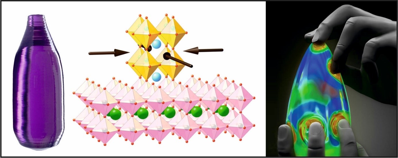
The goal of this collaboration is to achieve thin films of complex oxides with drastically improved electronic properties or that exhibit spectacular phenomena. Our approach is to target systems for study where appropriate substrates are needed to enhance properties or unleash novel phenomena in the overlying complex oxide film. The electronic properties and phenomena of interest include superconductivity, ferroelectricity, ferromagnetism, antiferromagnetism, piezoelectricity, pyroelectricity, multiferroicity, metal-insulator transitions, catalysis, electrical mobility, high spin polarization, thermoelectricity, non-linear optical, magnetoelectric, magneto-optic, and magnetothermal effects. Complex oxides are record holders for many of these behaviors. In many cases thin films with properties comparable to a desired complex oxide in bulk form have not been achieved because of the lack of an appropriate substrate, for example, when there are no commercial isostructural substrates with good lattice match.
This is the case for many perovskites, pyrochlores, magnetoplumbites and many other complex oxides, where there are no commercial substrates whatsoever with these structures. Our collaboration includes both types of substrate needs: more ideal substrates for the stable polymorph of complex oxides with stellar properties that have not been achieved in thin film form and substrates enabling the growth of metastable polymorphs of oxides. The latter approach was verified by a joint experiment published by Haeni et al. (2004) that ignited a fury of research in the strain-engineering of complex oxides.
Leibniz-Institut für Kristallzüchtung (IKZ):
Coordination: Dr. Christo Guguschev
Section: Oxides & Fluorides / Substrate Crystals for Advanced Functional Oxides
Cornell University:
Coordination: Prof. Darrell G. Schlom
Herbert Fisk Johnson Professor of Industrial Chemistry in the Department of Materials Science & Leibniz Chair at IKZ
Cornell Webpage: http://schlom.mse.cornell.edu/
Leibniz Chair: https://www.leibniz-gemeinschaft.de/ueber-uns/international/leibniz-chairs.html
J. H. Haeni, P. Irvin, W. Chang, R. Uecker, P. Reiche, Y. L. Li, S. Choudhury, W. Tian, M. E. Hawley, B. Craigo, A. K. Tagantsev, X. Q. Pan, S. K. Streiffer, L. Q. Chen, S. W. Kirchoefer, J. Levy & D. G. Schlom
Room-temperature ferroelectricity in strained SrTiO3
Nature
DOI: https://doi.org/10.1038/nature02773
K.J. Choi, M.D. Biegalski, Y.L. Li, A. Sharan, J. Schubert, R. Uecker, P. Reiche, Y.B. Chen, X.Q. Pan, V. Gopalan, L.-Q. Chen, D.G. Schlom, and C.B. Eom
Enhancement of Ferroelectricity in Strained BaTiO3 Thin Films
Science
DOI: https://doi.org/10.1126/science.1103218
J.H. Lee, L. Fang, E. Vlahos, X. Ke, Y.W. Jung, L.F. Kourkoutis, J-W. Kim, P.J. Ryan, T. Heeg, M. Roeckerath, V. Goian, M. Bernhagen, R. Uecker, P.C. Hammel, K.M. Rabe, S. Kamba, J. Schubert, J.W. Freeland, D.A. Muller, C.J. Fennie, P. Schiffer, V. Gopalan, E. Johnston-Halperin, and D.G. Schlom
A Strong Ferroelectric Ferromagnet Created by means of Spin-Lattice Coupling
Nature
DOI: https://doi.org/10.1038/nature10219
D. G. Schlom, L. Chen, C. J. Fennie, V. Gopalan, D. A. Muller, X. Pan, R. Ramesh and R. Uecker
Elastic strain engineering of ferroic oxides
MRS BULLETIN
DOI: https://doi.org/10.1557/mrs.2014.1
N.M. Dawley, E.J. Marksz, A.M. Hagerstrom, G.H. Olsen, M.E. Holtz, V. Goian, C. Kadlec, J. Zhang, X. Lu, J.A. Drisko, R. Uecker, S. Ganschow, C.J. Long, J.C. Booth, S. Kamba, C.J. Fennie, D.A. Muller, N.D. Orloff, and D.G. Schlom
Targeted Chemical Pressure Yields Tunable Millimetre-Wave Dielectric
Nature Materials
DOI: https://doi.org/10.1038/s41563-019-0564-4
C. Guguschev, D. Klimm, M. Brützam, T.M. Gesing, M. Gogolin, H. Paik, A. Dittmar, V.J. Fratello, D.G. Schlom
Single crystal growth and characterization of Ba2ScNbO6 – A novel substrate for BaSnO3 films
DOI: https://doi.org/10.1016/j.jcrysgro.2019.125263
A patent application is ongoing (US reference number: 16/424,987)


Joint Laboratory for Novel 2D Materials Synthesis and Electron Spectroscopy – JL-2DSES
To foster the longstanding collaboration between the Leibniz-Institut für Kristallzüchtung (IKZ) and Prof. Dr. Norbert Koch, Humboldt-Universität zu Berlin, both set up the ‘Joint Laboratory for Novel 2D Materials Synthesis and Electron Spectroscopy - JL-2DSES’ on the Adlershof campus in 2024. The aim of JL-2DSES is to provide state-of-the-art materials synthesis and electron spectroscopy infrastructure for solid-state physics and materials science on novel two-dimensional (2D) materials. The focus lies on molecular beam epitaxy (MBE) for the generation of extremely thin crystalline (hetero)structures and photoelectron spectroscopy (PES) as a surface-sensitive method of chemical and band structure analysis.
The JL-2DSES offers a unique research environment for university and non-university research institutions on the Adlershof campus and in Berlin. In addition to the opportunity to cooperate with partners in the field of materials and device production, new perspectives for interdisciplinary approaches to materials synthesis and characterization emerge. The JL-2DSES is intended to be a point of contact for scientific institutions and industry for questions relating to the electron spectroscopy of modern electronic materials, particularly in the fields of electronics, optoelectronics and photonics, as well as the synthesis of 2D materials. JL-2DSES is designed for the long term with the intention to coordinate in the best possible way the complementary human and material resources available to the IKZ and the HU while generating synergies for research, teaching and training.
IKZ-IRIS Joint Lab „Layer Transfer für 2D-Heterostrukturen“
The continued development of functional quantum materials is a demanding task with high priority for material science and applied research. Among existing quantum materials, 2D-materials possess outstanding opportunities. Yet, the full potential of exploiting their functionalities is only revealed through novel heterostructures. It is exactly this goal of the strategic cooperation “layer transfer for 2D-heterostructures”.
In principle, layer transfer allows the combination of crystalline materials without thermodynamic, kinetic or geometric constraints (lattice mismatch, crystal symmetry, combination of different thermodynamic phases, (de-)wetting properties), limiting classical bulk crystal growth or thin film epitaxy. In this way, layer transfer could set a new paradigm in fabricating innovative crystalline heterostructures with tailor-made properties. In particular for 2D-crystals such as graphene, transition metal di-chalcogeneides (TMDC) or hexagonal boron nitride (hBN), it has been demonstrated that specific material properties could be achieved merely by particular way of stacking order and orientation of individual layers. Such artificial heterostructures can often only be realized via layer transfer and not via established crystal growth. Therefore, layer transfer has established itself as a new "bottom-up" method for the construction of novel "2D goes 3D" materials and represents a fundamentally new synthesis path of crystalline materials.
We see our strategic cooperation "Layer transfer for 2D heterolayers" as an integral part of the overarching efforts towards material sovereignty and we aim to make a significant contribution to the development of quantum materials in the Berlin area.
A successful cooperation is promised by the complementary expertise of the Layer Transfer working group of Dr. Martin and the AG HYD of Prof. List-Kratochvil, which offers natural synergy effects and an ideal basis for scientific exchange and the development of new research projects.
Leibniz-Institut für Kristallzüchtung (IKZ)
Coordination: Dr. Jens Martin
https://www.ikz-berlin.de/forschung-lehre/nanostrukturen-schichten/sektion-halbleiternanostrukturen#c1493
IRIS-Adlershof
Coordination: Dr. Sylke Blumstengel
Hybrid Devices Group, Institut für Physik, Institut für Chemie & IRIS Adlershof
http://www.hyd.iris-adlershof.de/

Support Lab: Crystal Machining
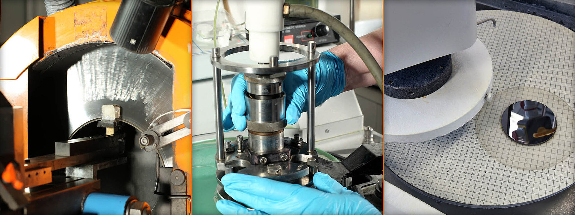
At the IKZ, crystals (Si, Ge, GaAs, InP, oxides, fluorides, AlN) with very different, in particular mechanical, properties are produced and have to be processed into tailor-made samples as preparation for different characterization methods.
For structural and optical characterization, wafers or longitudinal sections with polished surfaces are typically produced and then etched or irradiated. For the production of the required surface quality, several laboratory polishing machines are available on which polishing can be carried out with different polishing agents using purely mechanical but also chemical-mechanical processes. For laser applications, 3D samples are also required for which exact angles of the sample surfaces to each other must be realized. In addition to precise sawing and polishing machines, x-ray and laser measuring devices are available for this purpose, with which the samples can be precisely aligned before processing.
On request, the IKZ also offers processing services for external customers for the materials mentioned above.
Contact

Support Lab: Test structure lab
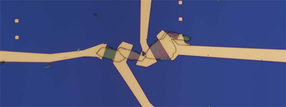
To bridge the gap between crystal characterization and prototype development, we are fabricating test devices from epitaxial thin films and microscopic 2D-crystals for electrical characterization. We employ electron beam lithography and direct laser writing for microscopic patterning, while metal contacts are produced by standard evaporation techniques. The test structure lab is operated in collaboration with Prof. E. List-Kratochvil, Center for the Science of Materials Berlin (CSMB), Humboldt University, Berlin.
Thin films are often employed in devices in which large electric fields are present and where local defects can affect device performance drastically. Microscopically small contacts minimize the chances of device failure and provide good statistics. Another application of lithography is the electrical characterization of exfoliated 2D-crystals as they have only microscopic lateral dimensions. Due to the irregular shape of the crystals, contact patterns must be designed individually.
Hao Chen, Pinjia Zhou, Jiawei Liu, Jiabin Qiao, Barbaros Oezyilmaz, Jens Martin
Gate controlled valley polarizer in bilayer graphene
Nature Communications
DOI: 10.1038/s41467-020-15117-y
Contact

Support Lab: ERDF Application Laboratory "Materials for Oxide Electronics”
Since March 2017, the ERDF Application Laboratory has been pursuing the goal of developing oxide functional layers with high structural perfection for application-relevant device test structures like for example semiconducting gallium-oxide layers (Ga2O3) for vertical power devices, resistively switchable strontium-titanate layers (SrTiO3) for ReRAMs and piezoelectric potassium-sodium-niobate layers ((K,Na)NbO3) for acoustic surface wave sensors.
This includes the deposition and characterization of single-crystalline, oxide layers with low defect density and defined electrical and structural properties tuned by doping and lattice strain. In order to achieve a high structural perfection of the layers, the section "Thin Oxide Films" uses the method of metal-organic vapor phase epitaxy (MOVPE), which is already the deposition method of choice in industry due to its scaling potential. In the application laboratory we are looking for synergies especially with regional academic and industrial partners.
Contact

Support Lab: Chemical Analysis
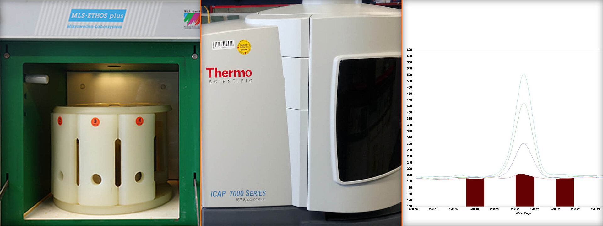
For the reliable evaluation of crystal growth and doping/impurities, regular measurement of the chemical compositions of both starting materials and crystal products is required. Our chemical analysis lab performs bulk and trace element analysis using ICP-OES instrument (applicable top most elements) and dedicated trace analysis of H, C, N, O and S using dedicated inert gas analysis instruments.
Chemical analysis is primarily performed with Inductively Coupled Plasma Optical Emission Spectroscopy (ICP-OES) and x-ray fluorescence analysis (XRF). Prior to the ICP-OES measurement, the materials to be measured must first be dissolved (digested) using a suitable method, which must be developed specifically for each material. XRF measurements are mainly used for the mapping of the chemical composition with a resolution of 25 µm. The core competence of IKZ is the measurement of oxide (e.g. Ga2O3, REScO3) and fluoride (e.g. CaF2, BaMgF4) materials.
On request, the IKZ also offers measurement services for external customers.
Contact