Young careers at IKZ

Scientific careers

The IKZ provides high-level education with a deep understanding of scientific concepts, essential to be competitive in the academic world. On the other hand, the IKZ offers possibilities for students and young scientists to broaden their field of expertise and develop various skills to pursue alternative career paths successfully. In the following, PhD students and PostDocs introduce themselves and describe their fields of research and interests that they engage in at IKZ.

Our young scientists
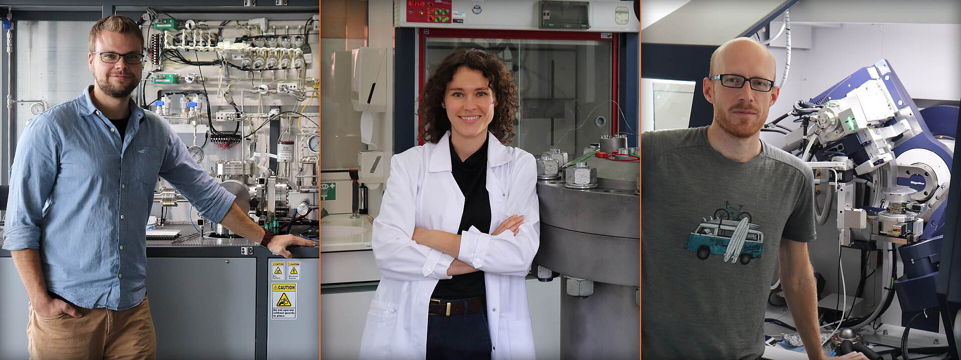
Ta-Shun Chou

Ta-Shun received his bachelor degree in materials science and chemistry at National Tsing Hua University in Taiwan. After his master studies at University Erlangen-Nuremberg, he joined Cynora GmbH as a Senior Process Engineer.

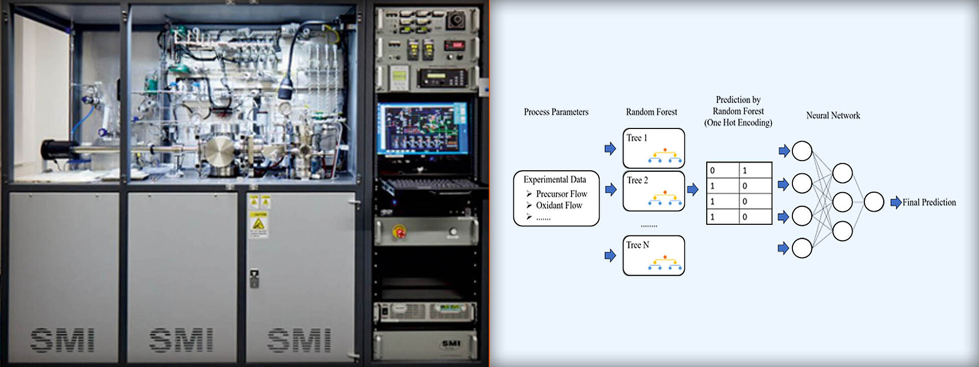
During his Ph.D. project, he aims to develop a MOVPE process of homoepitaxially grown ß-Ga2O3 for the industrial applications. He had implemented machine learning technique to accelerate the process development and had developed specific algorithm combining reflectance spectroscopy to in-situ monitor the growth process.

If you are interested in his research, please visit his research gate website or contact him on LinkedIn.

Section: Thin Oxide Films / Junior Research Group "Epitaxy of semiconducting Gallium Oxide"

ResearchGate: researchgate.net/profile/Ta-Shun-Chou
LinkedIn: linkedin.com/in/ta-shun-chou/

T.-S. Chou, P. Seyidov, S. Bin Anooz, R. Grüneberg, T. Thi Thuy Vi, K. Irmscher, M. Albrecht, Z. Galazka, J. Schwarzkopf, A. Popp
Fast homoepitaxial growth of (100) β-Ga2O3 thin films via MOVPE process
AIP Adv. 11 (2021) 115323
https://doi.org/10.1063/5.0069243

T.-S. Chou, S. Bin Anooz, R. Grüneberg, K. Irmscher, N. Dropka, J. Rehm, T.T.V. Tran, W. Miller, P. Seyidov, M. Albrecht, A. Popp
Toward Precise n-Type Doping Control in MOVPE-Grown β-Ga2O3 Thin Films by Deep-Learning Approach
Crystals. 12 (2022) 8
https://doi.org/10.3390/cryst12010008

S. Bin Anooz, R. Grüneberg, T.S. Chou, A. Fiedler, K. Irmscher, C. Wouters, R. Schewski, M. Albrecht, Z. Galazka, W. Miller, J. Schwarzkopf, A. Popp
Impact of chamber pressure and Si-doping on the surface morphology and electrical properties of homoepitaxial (100) β-Ga2O3 thin films grown by MOVPE
J. Phys. D. Appl. Phys. 54 (2021) 034003
https://doi.org/10.1088/1361-6463/abb6aa

K. Tetzner, K. Egbo, M. Klupsch, R.-S. Unger, A. Popp, T.-S. Chou, S. Bin Anooz, Z. Galazka, A. Trampert, O. Bierwagen, J. Würfl
SnO/β-Ga2O3 heterojunction field-effect transistors and vertical p–n diodes
Appl. Phys. Lett. 120 (2022) 112110
https://doi.org/10.1063/5.0083032

Contact
Ta-Shun Chou

Kontakt Ta-Shun Chou

Ph. +49 30 6392 2846

Arved Enders-Seidlitz

Arved works since July 2020 as PhD student in the NEMOCRYS project of the group Model Experiments at the IKZ. His topic is the development and validation of multiphysical computer simulations for crystal growth processes using open source software. If you are interested in his research visit his research gate website or contact him on LinkedIn.

Section Fundamental Description, Junior Research Group "Model experiments"

ResearchGate: researchgate.net/profile/Arved_Enders-Seidlitz2
LinkedIn: linkedin.com/in/arved-enders-seidlitz-465830176/

Kontakt
Arved Enders-Seidlitz

Arved Enders-Seidlitz

Ph. +49 30 6392 3129

Anastasiia Kochan (Uvarova)

Anastasiia's mission is to develop gain materials for lasers with emission wavelengths in the 1 µm and 3 µm spectral range. Both are of high interest and possess a wide range of applications in materials processing, medical treatment and environmental monitoring. In particular cubic sesquioxide crystals enabled excellent laser performance when doped with Yb3+ and Er3+. However, the growth of sesquioxides is very challenging due to their high melting temperatures of more than 2400°C.

Her current activities include the development of a growth process for high quality rare-earth doped laser by the optical floating zone method (OFZ), the spectroscopic investigation of these crystals and to perform basic laser experiments.
During OFZ growth, a ceramic rod is molten by intense light and solidifies in form of a single crystal. As the molten zone is held together by surface tension, it avoids the use of expensive noble metal crucibles and insulations and enables a free choice of the growth atmosphere without restrictions imposed by crucible and insulation.
Our initial spectroscopic results reveal superior properties of OFZ crystals as compared to previous crystals grown from rhenium crucibles by the heat exchanger method (HEM) and corresponding laser experiments will be performed in the near future.

Section Crystalline Materials for Photonics, Center for Laser Materials

Xing: xing.com/profile/Anastasia_Uvarova2/
LinkedIn: linkedin.com/in/anastasia-uvarova

Contact
Anastasiia Kochan (geb. Uvarova)

Kontakt Anastasiia Kochan (geb. Uvarova)

Ph. +49 30 6392 3122

Yujia Liu

After study in material science in university Ulm, Yujia works in IKZ on SiGe-based material for qubit devices. She has been working on isotopically engineered epitaxy as well as heterostructure characterization. On the way to push Si and Ge such classical semiconductor into quantum information age, the requirements of SiGe heterostructure crystal perfection are leveled - such as atomic steps on the interface, local strain relaxation, local tilt in the strained thin Si layer should be reduced to extend the coherence time of confined electron spin as much as possible. To develop high performance quantum computer is a multidisciplinary task including material science.

Before Yujia’s research adventure in group IV semiconductor, she also worked on III-V materials AlN and GaN as well as II-VI material ZnO.

Section: Semiconductor Nanostructures

LinkedIn: linkedin.com/in/yujia-liu-940824/

Contact
Yujia Liu

Yujia Liu

Ph. +49 30 6392 3055

Pradeep Chandra Palleti

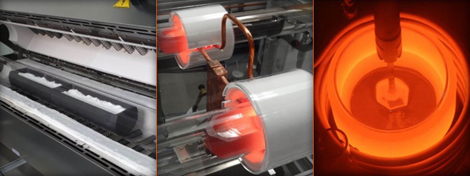
After finishing his studies in crystalline materials at University of Freiburg, he started working at the IKZ on high purity germanium for gamma radiation detectors. HPGe is the best material due its purity and the fact that it has less electrical active defects than any other solid material. He has been working on reduction of germanium dioxide to germanium. The germanium obtained from reduction is zone refined to remove the impurities and HPGe crystals were grown using Czochralski method. Electrical resistivity, Hall effect measurements on HPGe crystals (20-300K), PTIS(7K), etch pit density analysis, and carrier lifetime measurements with MDP were performed to understand the electrical properties of HPGe. He is proud to be a member of the LEGEND collaboration.

Section: Semiconductors, Group: Cz-IV

LinkedIn: linkedin.com/in/pradeep-chandra-palleti

Contact
Pradeep Chandra Palleti

Pradeep Chandra Palleti

Ph. +49 30 6392 2896

Palvan Seyidov

Gallium oxide (Ga2O3) is emerging as a viable candidate for certain classes of power electronics, solar blind UV photodetectors, solar cells, and sensors with capabilities beyond existing technologies due to its large bandgap. Palvan´s scientific interest include the charge and spin transport physics of device related gallium oxide (Ga2O3) bulk crystals and homoepitaxial layers. To understand the electrical properties of gallium oxide crystals grown at the IKZ, he uses conductivity and Hall effect measurements (20-1100K), deep-level transient and optical  spectroscopy (20-800K) as well as for optical characterization he uses transmission / reflection spectrometers in the wavelength range from 120nm to 100um and micro-Raman spectrometer with 6 excitation wavelengths (325-785 nm).

Section Experimental Characterization

LinkedIn: linkedin.com/in/palvan-seyidov-640708187

Contact
Palvan Seyidov

Palvan Seyidov

Ph. +49 30 6392 3086

Lucas Vieira

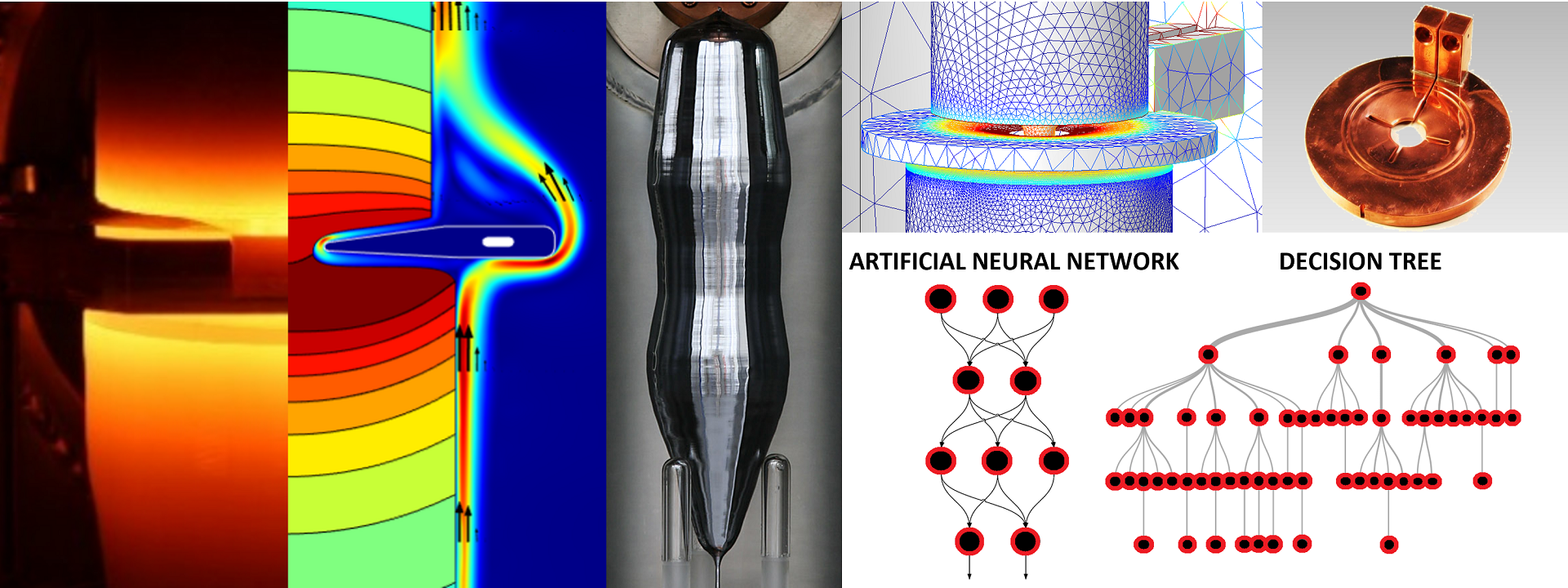
Lucas holds a double degree in Mechanical and Materials Engineering from a Franco-Brazilian cooperation program. During his master thesis, he developed a finite element model of the quench phenomenon in superconducting magnets for particle accelerators. His experience with multiphysics simulations is now in use at the IKZ for modelling Si growth via the Float Zone method. Once robust and validated models are obtained, they will be used to train Neural Networks and optimize growth parameters. Machine learning is expected to significantly help overcome current challenges in growing 8-inch Float Zone Si crystals.

Section: Fundamental Description / Numerical Simulation

LinkedIn: linkedin.com/in/lrvieira/en

Contact
Lucas Vieira

Lucas Vieira

Ph. +49 30 6392 3063