Section Semiconductor Nanostructures
Section Semiconductor Nanostructures
Mission
In our section we develop materials and methods for innovative Semiconductor Nanostructures for future technologies. Crystalline thin films are important components of state-of-the-art electronic and optoelectronic devices and drivers of innovations.
With recently emerging applications such as quantum computation, new challenges arise in thin film processing to meet increased demands on material qualities, such as isotopic purification or strain engineering. Complimentary, the novel thin film assembly technique “layer transfer” promises a paradigm change in the way we can create functional interfaces and heterostructures, and ultimately artificial crystalline structures: “2D goes 3D”.
Research activities
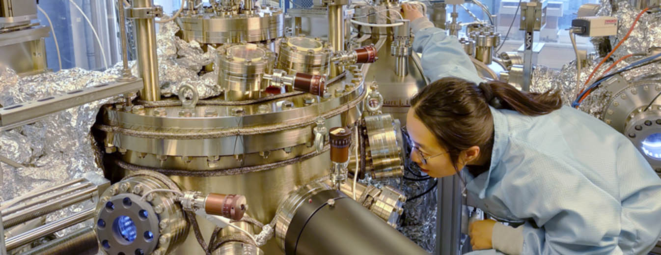
We employ a range of different growth principles and concepts, including molecular beam epitaxy (MBE) and chemical vapour deposition (CVD), to control nucleation and lateral growth, to form homo- or heterogenous interfaces and to suppress or to specifically trigger defect formation. We utilize especially designed equipment such as an MBE system for the deposition of ultrapure 28Si layers and 76Ge, a CVD system with laser-assisted local nucleation as well as dedicated furnaces for the growth of 2D-van der Waals materials.
A high vacuum layer transfer station allows stacking of thin crystalline films on custom target substrates. A particular research focus lies in the development of “quantum materials” for electronic spin-qubits or single photon sources.
Head of section

Topics
Junior Research Group "SiGe-based Quantum Materials and Heterostructures"
The future potential of quantum technology and especially quantum computing is very high. SiGe heterostructures thereby constitute one of the most promising material platforms, since they combine high crystalline perfection and purity with potentially easy scalability, and the possibility to create a spin-neutral environment for quantum dots by isotopic enrichment.
The IKZ combines the competence and experience in processing isotopically enriched semiconductor materials such as 28Si, 72Ge, and 76Ge to supply high-quality quantum materials.
The research of our group focuses on the growth of SiGe-based heterostructures by molecular beam epitaxy (MBE) and their characterization for the application in quantum technology. We are specialized in nuclear spin-free SiGe/Si/SiGe and SiGe/Ge/SiGe heterostructures for spin qubits, as well as Si/SiO2 structures (Silicon on Insulator, SOI) for optical quantum emitters. The scientific interest centers upon obtaining preferably atomically flat interfaces, the realization of low dislocation densities, as well as the control of chemical impurities.
Liu, Y., Gradwohl, K.P., Lu, C.H., Dadzis, K., Yamamoto, Y., Becker, L., Storck, P., Remmele, T., Boeck, T., Richter, C. and Albrecht, M., 2023.
Strain relaxation from annealing of SiGe heterostructures for qubits.
Journal of Applied Physics, 134(3).
DOI: 10.1063/5.0155448
Liu, Yujia, Kevin-Peter Gradwohl, Chen-HSun Lu, Yuji Yamamoto, Thilo Remmele, Cedric Corley-Wiciak, Thomas Teubner, Carsten Richter, Martin Albrecht, and Torsten Boeck.
Growth of 28Si Quantum Well Layers for Qubits by a Hybrid MBE/CVD Technique.
ECS Journal of Solid State Science and Technology 12, no. 2 (2023): 024006.
DOI:10.1149/2162-8777/acb734
Gradwohl, Kevin-P., Chen-Hsun Lu, Yujia Liu, Carsten Richter, Torsten Boeck, Jens Martin, and Martin Albrecht.
Strain relaxation of Si/SiGe heterostructures by a geometric Monte Carlo approach.
physica status solidi (RRL)–Rapid Research Letters 17, no. 6 (2023): 2200398.
DOI: 10.1002/pssr.202200398
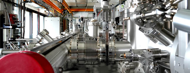
Thin film growth by molecular beam epitaxy at Leibniz-Institut für Kristallzüchtung

2D van der Waals materials and Layer Transfer
A new paradigm to assemble crystalline materials is established by layer transfer, a method to build-up novel functional crystalline heterostructures which cannot be grown by traditional epitaxial methods due to incompatibility of lattice parameters, symmetry, or others. We are aiming for a comprehensive and flexible technical approach to facilitate the realization of various demands in basic and applied research, seeking synergies with local academic and industrial partners.
We target the epitaxial growth of 2D van der Waals materials on wafer-scale (up to 2”), combining the advantages of different thin film growth techniques. With a layer transfer station, which can be operated remotely under high vacuum conditions, the epitaxial films and exfoliated monolayers of 2D-crystals can be transferred on a specific target wafer in a precisely controlled stacking sequence.
In basic research, a special interest is in emergent phases such as strongly correlated electronic matter in 2D-heterostructures. Reliable single photon emitters for quantum applications are also in high demand. In applied research, high performance systems can be realized by the combination of the best materials for the best function in a hybrid approach.
Rongbin Wang, Martin Schmidbauer, Norbert Koch, Jens Martin, and Sergey Sadofev.
Y‐Stabilized ZrO2 as a Promising Wafer Material for the Epitaxial Growth of Transition Metal Dichalcogenides.
physica status solidi (RRL)–Rapid Research Letters 18, no. 1 (2024): 2300141.
DOI: 10.1002/pssr.202300141
Rongbin Wang, Norbert Koch, Jens Martin, and Sergey Sadofev.
Recrystallization of MBE‐Grown MoS2 Monolayers Induced by Annealing in a Chemical Vapor Deposition Furnace.
physica status solidi (RRL)–Rapid Research Letters 17, no. 5 (2023): 2200476.
DOI: 10.1002/pssr.202200476
Hao Chen, Pinjia Zhou, Jiawei Liu, Jiabin Qiao, Barbaros Oezyilmaz, Jens Martin
Gate controlled valley polarizer in bilayer graphene
Nature Communications
DOI: 10.1038/s41467-020-15117-y
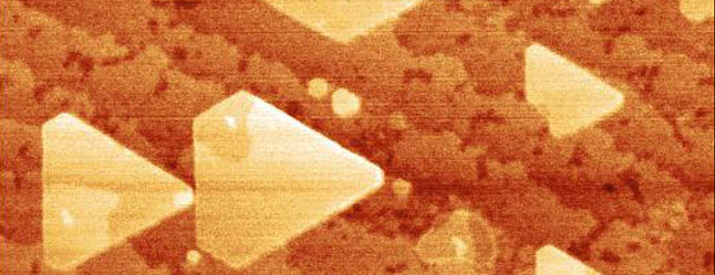
Topographic Atomic force micrograph (AFM) of epitaxial 2D-WS2 on sapphire