Section Crystals for Electronics
Section Crystalline Materials for Electronics
Mission
Our aim is to produce small series of prototype substrates with tailored properties from semiconductor crystals with promising properties and to make these available to research partners to enable innovation in epitaxial and device processes or new applications. This requires not only the optimization of crystal growth and preparation processes with regard to technological capability, but also the development of standardized and efficient characterization methods for each specific material.
Research activities
For the key materials AlN and Ga2O3 with an extremely large band gap (ultra-wide band gap: UWBG), efficient and reproducible crystal growth and machining processes are to be developed for the production of prototype semiconductor substrates with diameters of up to 2” and beyond. The scientific focus is on structural defects and their avoidance as well as point defects (O, C, Si), which have a decisive influence on volume properties such as optical absorption and electrical conductivity.
The Micro-Structuring and Transfer working group aims to integrate these and other high-performance but expensive semiconductor materials as single-crystal µ-substrates into existing Si platforms.
The section also operates the “Crystal Machining” support lab.
Head of section

Topics
Aluminum Nitride Prototyping
Single-crystalline aluminium nitride is a promising substrate material for the production of ultraviolet light-emitting diodes (UV LEDs), which are used for disinfection, ultraviolet laser diodes (UV LDs), which are used for medical metrology applications and next-generation power electronics components. We produce AlN substrates with low dislocation densities, high UV transparency and high surface quality so that project partners can use them to develop new components.
Aluminium nitride (AlN) crystals are grown via physical vapor transport (PVT) in crucibles made of TaC or W and must have low dislocation densities and relevant diameters (>= 1") regardless of the planned application. Prerequisites for the production of AlN crystals with high crystalline quality are the availability of low-defect seeds, the avoidance of impurity precipitation during heating and an optimal T-field design (e.g. high T, low T gradients).
The increase in diameter is achieved by a gradual increase of seed diameters in several successive growth runs with suppression of parasitic growth and slow lateral growth by means of suitable lateral T-gradients. For use as a substrate for UV emitters, sufficient transparency is required in the desired wavelength range, which can be adjusted as required by specifically influencing the concentrations of the main impurities O, C and Si. Electrically conductive substrates for the production of vertical power electronics components are not yet available and the IKZ has set itself the goal of systematically investigating the underlying physical processes in order to realize n-conductive substrates technologically in case of success.
Carsten Hartmann, Merve Pinar Kabukcuoglu, Carsten Richter, Andrew Klump, Detlev Schulz, Uta Juda, Matthias Bickermann, Daniel Hänschke, Thomas Schröder, and Thomas Straubinger
Efficient diameter enlargement of bulk AlN single crystals with high structural quality
Applied Physics Express 16 (7), 075502 (2023)
DOI: 10.35848/1882-0786/ace60e
Thomas Straubinger, Carsten Hartmann, Merve P. Kabukcuoglu, Martin Albrecht, Matthias Bickermann, Andrew Klump, Simon Bode, Elias Hamann, Simon Haaga, Mathias Hurst, Thomas Schröder, Daniel Hänschke, and Carsten Richter
Dislocation Climb in AlN Crystals Grown at Low-Temperature Gradients Revealed by 3D X-ray Diffraction Imaging
Crystal Growth & Design 23 (3), 1538 (2023)
DOI: 10.1021/acs.cgd.2c01131
Andrew Klump, Carsten Hartmann, Matthias Bickermann, and Thomas Straubinger
Prediction of impurity concentrations in AlN single crystals by absorption at 230 nm using random forest regression
CrystEngComm 27 (2), 184 (2025)
DOI: 10.1039/d4ce00813h
![[Translate to English:]](/fileadmin/_processed_/5/c/csm_T_AlN_Kristallzuechtung_3118fb9092.jpg "[Translate to English:]")
Left: Facilities for growing AlN single crystals at IKZ; Middle: View into the sublimation growth facility; Right: AlN single crystal

Gallium Oxide Prototyping
Single crystalline gallium oxide with its large band gap (4.5 - 4.8 eV) and high breakdown field (8 MV/cm) is a promising substrate material for the fabrication of efficient next generation power electronic devices. We produce low-defect gallium oxide substrates with 2” diameter, different orientations and defined off-cuts for project partners to develop new lateral (semi-insulating) or vertical (conductive) power electronic devices.
The central target of the group is to develop reproducible CZ crystal growth processes for the production of low-defect semi-insulating (Mg:) and conductive (Si:) gallium oxide crystals with diameters of at least 2” and lengths greater than 50 mm. This development is to be supported by basic research on structural defects (foreign grains, twin envelopes, dislocations) together with the Materials Science Department. In parallel, in-house machining processes are to be developed for the efficient and cost-effective production of 2” substrates. The focus here is on sawing the easily cleavable crystals with off-cut and producing the 100-X° and 010-X° substrate orientations.
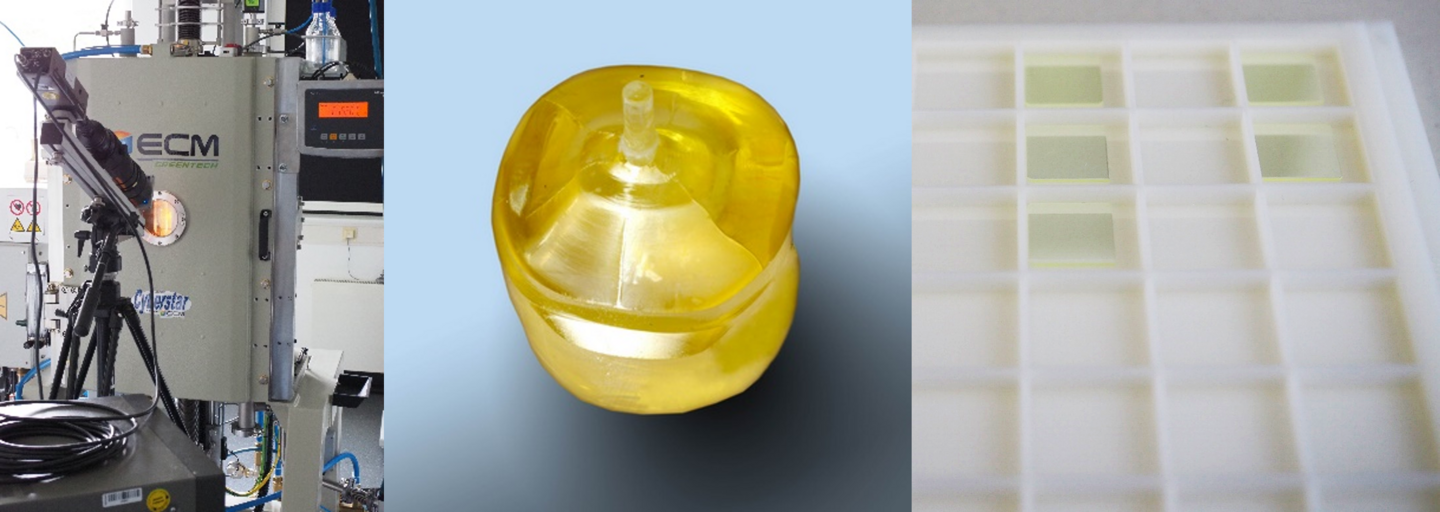
Left: CZ system for growing Ga₂O₃ single crystals at the IKZ; center: Mg-doped 2” Ga₂O₃ crystal; Right: Ga₂O₃ substrates
Gallium Oxide Epitaxy
Modern society relies on a wide range of electrical and electronic systems. To achieve this, the conversion of electrical energy must be carried out as efficient as possible. The material system β-Ga2O3 has due to its high bandgap of approx. 4.8 eV and the resulting theoretically high breakdown field strength the best prerequisites to become the high-performance material for next generation power applications. Therefore our mission is to achieve the predicted material properties through process development to pave β-Ga2O3 the way into power electronics.
The β-Ga2O3 MOVPE process development is focused on the investigation of the effects of the growth parameters and the type of doping on the electrical properties of the layers. Another focus is the homoepitaxial growth on differently oriented substrates and the influence on the generation of crystal defects. In addition, there are studies on increasing the growth rate by maintaining the good layer quality. In order to improve the positive properties of Ga2O3 even further the material is alloyed with Aluminum.
Offer: Gallium oxide substrates and epi-layers
Download Flyer: „Gallium Oxide – The Next High Performance Material for High Power Devices“
IKZ Online Lecture: Dr. Andreas Popp: "β-Ga2O3: The Next Material for High Power Electronics?"
S. Bin Anooz, R. Grüneberg, C. Wouters, R. Schewski, M. Albrecht, A. Fiedler, K. Irmscher, Z. Galazka, W. Miller, G. Wagner, J. Schwarzkopf and A. Popp
Step flow growth of β-Ga2O3 thin films on vicinal (100) β-Ga2O3 substrates grown by MOVPE
Appl. Phys. Lett.116, 182106 (2020)
DOI: 10.1063/5.0005403
T.-S. Chou, P. Seyidov, S. Bin Anooz, R. Grüneberg, J. Rehm, T.T.V. Tran, A. Fiedler, Z. Galazka, M. Albrecht, and A. Popp
High-mobility 4 μm MOVPE-grown (100) β-Ga2O3 film by parasitic particles suppression
Jpn. J. Appl. Phys. 62, SF1004 (2023). [Spotlight Article]
DOI: 10.35848/1347-4065/acb360
T.-S. Chou, P. Seyidov, S. Bin Anooz, R. Grüneberg, M. Pietsch, J. Rehm, T.T.V. Tran, K. Tetzner, Z. Galazka, M. Albrecht, K. Irmscher, A. Fiedler, and A. Popp
Suppression of particle formation by gas-phase pre-reactions in (100) MOVPE-grown β-Ga2O3 films for vertical device application
Appl. Phys. Lett. 122, 052102 (2023).
DOI: 10.1063/5.0133589
![[Translate to English:]](/fileadmin/user_upload/Forschung_Lehre/Abteilung_Nanostrukturen_Schichten/Sektion_Duenne_Oxidschichten/T_Ga2O3.jpg "[Translate to English:]")
Gallium oxide substrates

GOAL – Gallium Oxide Application Laboratory for Power Electronics
With the project G.O.A.L. (“Gallium Oxide Application Laboratory for Power Electronics”), led by Dr. Andreas Popp, the Leibniz-Institut für Kristallzüchtung (IKZ) is expanding its research and development infrastructure in the field of innovative semiconductor materials. The aim of the project is to establish an integrated technological platform for the semiconductor material gallium oxide (Ga₂O₃) for applications in power electronics.
IKZ has extensive expertise in the growth of gallium oxide bulk crystals as well as in substrate and wafer processing. Within the framework of the project, this existing infrastructure is being systematically expanded to include the process step of gallium oxide epitaxy.
Gallium oxide-based power electronics addresses a wide range of application fields. New markets are emerging particularly at the level of semiconductor technologies (wafers, transistors, power modules) and through increased value creation in the electronics industry, especially in power electronic converters for applications such as e-mobility, photovoltaics, wind energy, and power plant transformation. Improved material properties enable reduced energy losses and increased system efficiency, thereby supporting the energy transition. To enable industrial applications and the development of electronic devices, wafer layer systems with diameters of at least 2 inches are required.
A key investment focus of the project is therefore the installation of a 3×2" MOVPE system from AIXTRON for the deposition of epitaxial gallium oxide layers on wafers up to 4 inches in diameter. The system includes an integrated in-situ monitoring system from LayTec, enabling continuous process monitoring and quality control during growth.
This investment establishes the technical basis for the production of 2- to 4-inch gallium oxide epitaxial wafers and thus enables the extension of the value chain at the site.
The acquisition of the MOVPE system, including the in-situ monitoring system, represents the core investment of the project. Without this expansion of technical infrastructure, made possible by the project, the implementation of the project objectives would not be feasible.
The project is co-financed by the European Regional Development Fund (Europäischer Fonds für regionale Entwicklung, EFRE). The funding supports the targeted expansion of application-oriented research infrastructure, strengthens innovation capacity, and advances technological competencies at the Berlin location.
In this way, the project contributes to strengthening the regional innovation ecosystem and enhancing competitiveness in the field of advanced semiconductor technologies.
The project is embedded in existing collaborations with partners from academia and industry, including the Ferdinand-Braun-Institut as well as other institutions and companies in the Berlin-Brandenburg region.
With G.O.A.L., IKZ aims to establish itself as a Europe-wide research partner and supplier of 2-inch gallium oxide epitaxial wafers as a base material for power electronic devices. Due to the strong industrial relevance, direct exploitation in the semiconductor and power electronics industry (e.g., Bosch, Infineon, ZF) is expected. In addition, the IKZ Startup „NextGO-Epi“, founded in April 2025, is expected to significantly benefit from G.O.A.L. in terms of its development and market opportunities.
Micro-structuring & transfer
Semiconductor crystals of group III-V (e.g. InP, AlN) are substrate materials of the future for microelectronic, photonic, and opto-mechanical components that find applications in areas such as mobile communication, sensing, medical technology, and automotive. Integrating them into mature Si or sapphire-based technology platforms has the potential to realize cost-effective semiconductor devices with superior properties.
To enable this fundamentally new and future-oriented device generation, we want to develop preparation and transfer processes for integration on Si and other target substrates for III-V bulk crystals grown at the IKZ. Our activities are conducted in close collaboration with the bulk crystal growth (VGF-III-V, Aluminium Nitride Crystal Growth) and Wafering research groups, the IKZ-IRIS joint lab „Layer Transfer" as well as partners specialized in device development.
The R&D activities include:
- Preparation of InP and AlN single crystals with high crystalline perfection and tailored bulk properties (especially doping) into thin layers or micro-platelets with atomically smooth surfaces and low defect densities in preparation for the transfer.
- Optimization of the necessary chemical-mechanical polishing processes (surface) and lithography techniques (micro-structuring).
- Development of methods for characterizing the structural, optical, and electrical properties of the thin layers and micro-platelets.
- Development of transfer processes for the heterointegration of thin layers and micro-platelets onto Si substrates and other material platforms.
- Development of device demonstrators in collaboration with external project partners.
- Investigation of the influence of doping, micro-preparation, and bonding on crystal properties and device parameters.
- Adaptation and optimization of the developed methods for other application-relevant materials.
Isabella Peracchi, Carsten Richter, Tobias Schulz, Jens Martin, Albert Kwasniewski, Sebastian Kläger, Christiane Frank-Rotsch, Patrick Steglich, Karoline Stolze.
Preparation and Investigation of Micro-Transfer-Printable Single-Crystalline InP Coupons for Heterogeneous Integration of III-V on Si.
Crystals, 13 (7), 1126, 2023.
DOI: 10.3390/cryst13071126
![[Translate to English:]](/fileadmin/_processed_/f/5/csm_T_Mikro_Transfer_V1_00ada0087c.png "[Translate to English:]")
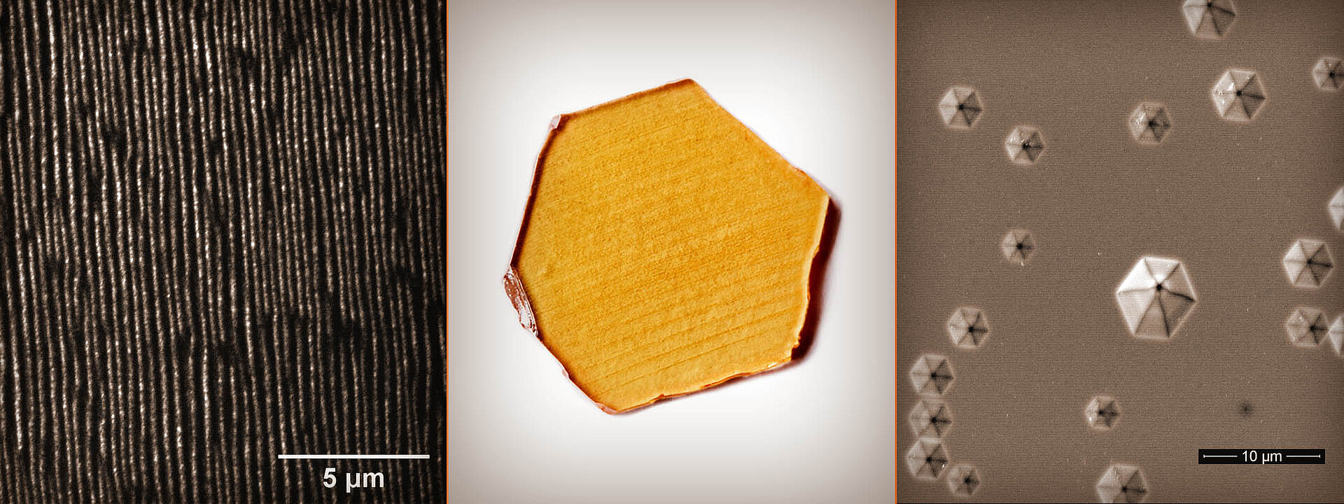
Process chain – from single crystal to III-V on Si integration; Left: III-V single crystals, 1’’ AlN and 4’’ InP; Centre left: 10 µm thin InP-layer with AFM image; Centre right: InP micro-platelets; Right: Schematic image of transferred micro-platelets on Si target substrate.

Wafering
At the IKZ the installation of a technology-ready processing line for the preparation and characterization of semiconductor substrates with diameters up to 2" is planned. Currently, the IKZ is already able to produce demonstrator substrates (e.g. aluminium nitride) with small diameters and high quality. For the production of prototypes and small series, the machining effort must be reduced and the process reproducibility must be improved.
Central technical or scientific challenges in the production of semiconductor substrates are:
- Low-loss sawing of crystals with different mechanical properties, especially of brittle materials.
- Precise orientation of crystals or substrates.
- Realization of a high structural surface quality through optimal polishing processes.
- Realization of a high surface purity by avoiding contamination during the machining processes and suitable final cleaning processes.
![[Translate to English:]](/fileadmin/_processed_/4/f/csm_T_Substratherstellung_f397b298a6.jpg "[Translate to English:]")
Left: Wire sawing; Middle: Substrates on polishing carrier; Right: TEM images of an AlN substrate surface after chemical-mechanical polishing - Top: Crystal volume near the surface (dark) in low magnification - Below: Near-surface ordered atomic structure without damage in high resolution