Service & Marketing
Services
Our service offers can be provided for research purposes or as individual items. In addition to research of new crystalline materials and the development of crystal growing technologies, we also offer expertise in characterization, equipment development, crystal processing and modelling.
We also provide our expertise as consultancy or expert opinions.
Contact

Based on our results from research, application-oriented knowledge and practical experience, we develop new technologies and processes for growing crystalline materials.
An overview of currently used methods and our portfolio of special equipment can be found here.
We offer support and advice in the following areas of development:
- Development of new growth methods and technologies
- Improvement of established growth methods
- Process investigations and process optimization
- Doping
- Material characterization
- Crystal processing technologies
In cooperation with our plant engineering facility, plants and their components are developed or modified for growth. One example is the development of the KristMAG® technology for crystal growth in the magnetic field, which was awarded the Berlin-Brandenburg Innovation Prize.
The IKZ has far-reaching expertise in the development of crystalline materials. We are pleased to provide our materials for research purposes.
Bulk cystals:
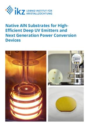
- Aluminium nitride bulk single crystals and solid solutions (also specifically doped)
- Gallium arsenide bulk single crystals (Vertical Gradient Freeze (VGF) using a KristMAG®-heater-magnet-module)
- Gallium arsenide crystals (according to customer-specific special requirements)
- Germanium crystals (also specifically doped)
- Oxides and fluorides crystals (according to customer-specific special requirements)
- Silicon ingots (multi-crystalline, high performance multi-crystalline, quasi-mono p- and n-type doped)
- Silicon germanium solid solutions (also specifically doped)
- Silicon crystals (also specifically doped)
Epitaxy:
- Copper indium gallium diselenide islands for micro-concentrator solar cells
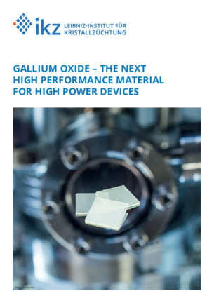
- Gallium or aluminium oxide layers (n-type, on Ga2O3, Al2O3 or Si)
- Polycrystalline silicon layers on glass or cost-effective substrates
- Niobium oxide layers
- Potassium sodium niobate layers
- Silicon / Germanium - Molecular beam epitaxy using both solid sources (MBE) and gaseous precursors (GSMBE)
- Silicon & Germanium nanostructures
- Strontium ruthenate layers
- Strontium titanate layers
The technological development of high-quality crystals as well as efficient crystal growing methods places high demands on the conception of the plant construction. At the Leibniz-Institut für Kristallzüchtung, these tasks are carried out by the equipment engineering group in close consultation with scientists.
The working group, consisting of engineers and technicians, has many years of sound knowledge in the field of scientific plant and equipment construction. It develops plant components that have not been commercially available so far and thus enables interesting new research approaches.
The main focus of our Equipment Engineering Group is on the following fields of activity:
- Professional consulting on technical questions of crystal growing
- Development, construction and modification of mechanical and electronic assemblies with resulting production-compatible documentation
- Repair, maintenance and professional reconstruction of crystal growth plant
The institute is one of the few research institutions with its own expertise in the field of plant engineering, which is why we are pleased to offer our services to external partners.
The Leibniz-Institut für Kristallzüchtung offers numerical modelling and feasibility studies as a service for external partners on request. Our range of services includes the following services:
- 2D and 3D modelling of temperature, Lorentz force and flow fields for the use of magnetic fields in crystal growing
- Calculation of thermal tensions in crystals
- Global simulation to optimize the growing process
- Fundamental studies on growth kinetics
- Design accompanying and process-supporting calculations for transport processes and field distributions in growth methods
- Feasibility studies for the development of technologies or the adaptation of growth systems in the portfolio of our partners
- Numerical modelling of heat and mass transport
- Numerical simulation of the PVT process
- Numerical investigations of crystal growth processes and methods
We offer expertise in the physical characterization of crystalline materials, investigation at the atomic level by electron microscopy as well as chemical and thermodynamical analysis.
We provide our expertise for research and development projects and offer consultations and measurements on request.
Microscopy:
- Atomic force microscopy (additional PFM and conductive-AFM)
- Confocal microscopy (CFM)
- Focused ion beam
- In-situ TEM (gas atmospheres up to 1 bar, T up to 1000 °C, biasing heating)
- Light microscopy
- Scanning electron microscopy (SEM) - analyses (mapping, EDX, EBSD, WDS)
- Scanning transmission electron microscopy (STEM-analyses, phase determination)
- Transmission electron microscopy (strain analyses)
Spectroscopy and optical imaging methods:
- Capacitance spectroscopy (DLTS incl. C-V/C-f/I-V)
- Cathodoluminescence (correlation of optical, electrical and structural properties)
- Electron paramagnetic resonance
- Ellipsometry
- HRTEM analyses, quantitative strain analysis, analysis of defects
- Infrared spectroscopic analysis of impurities
- Laser scattering tomography: Illustration of decorated dislocation networks over macroscopic crystal regions
- Lifetime measurement of silicon (MDPmap)
- Luminescence intensity distribution
- Measurement of the optical transmittance in the wavelength range from 120 nm to 3.3 µm
- Micro raman scattering
- Photoluminescence
- Photothermal ionization
- Si, Ge and SiGe sample measurements by (LPS) and photoluminescence (PL)
- Spectral transmission (up to 1600 °C)
- Transmittance / reflectance (VUV - FIR)
X-ray diffraction:
- Diffractometry (high-resolution)
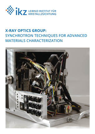
- Diffuse scattering using synchrotron radiation (ESRF, BESSY, DESY)
- Orientation of crystals
- Powder diffractometry
- Reflectometry
- Rocking curve analysis
- Texture determination
- X-ray determination of crystal orientation and crystal phases
- X-ray topography
Further characterization methods:
- Chemical analyses with ICP, ICP-OES and x-ray fluorescence (XRF)
- Conductivity measurements
- Determination of the electrical properties of semiconductor crystals
- Differential scanning calorimetry (DSC, up to 1650 °C)
- Differential thermal analysis (DTA/DG, in various atmospheres up to 2400 °C)
- Emanating gas analysis (EGA) up to 2000 °C
- FE tester for measurement of ferroelectric properties, with laser interferometer for determination of piezoelectric coefficients
- Growth and relaxation processes in the epitaxy
- Thermodynamic equilibrium calculations
- Thermogravimetry (TG)
We can offer service and research orders for industry, universities and other research institutions, ranging from the fabrication of machined samples to the development of technologies and related documentations. Special demands on geometry and surface quality of various samples can be fulfilled in short time and with high quality.
In cooperation with the characterization group we ensure a high quality standard.
Our portfolio includes the following services:
- Crystal cutting and wafering (single and multi-diamond wire, inner diameter diamond sawing)
- Surface grinding
- Lapping and polishing
- Mechanical and chemo-mechanical polishing
- Determination of geometrical parameters of the surface
![[Translate to English:]](/fileadmin/_processed_/d/8/csm_IKZ_Jahresbericht_2023_web__7163704e79.png "[Translate to English:]")
![[Translate to English:]](/fileadmin/_processed_/f/c/csm_IKZ_Jahresbericht_2022_web_ab9fe0b74f.png "[Translate to English:]")
![[Translate to English:]](/fileadmin/_processed_/4/4/csm_IKZ_Jahresbericht_2021_eecfff0715.png "[Translate to English:]")