Section Experimental Characterization
Section Experimental Characterization
Mission
The section agglomerates a comprehensive spectrum of tools to characterize the materials grown at the institute and of scientific partners. This is done as scientific service by providing fast feedback for crystal growers to improve their materials and with the aim to perform basic research in the field of solid-state physics and crystal growth. Our tools comprise structural, optical, electrical and thermoanalytical techniques; they cover all length scales from the macroscopic to the atomic scale. Combining these experimental techniques, we aim at an interdisciplinary effort at tackling urgent questions in solid state physics and at providing reliable materials parameters.
Research activities
The section is engaged in studying basic materials properties. This comprises electrical, optical and structural properties. We focus on semiconductors and dielectrics. Materials under study are III-Nitrides, Oxides and classical III-V- and group IV semiconductors. Doping, atomic defects, epitaxial heterostructures, growth and relaxation phenomena as well as optical properties are the most important topics. The section has strong collaboration with groups working in solid state theory. Recently we have a strong activity are developing in-situ characterization techniques in transmission electron microscopy and x-ray diffraction.
In addition, the section operates the joint laboratory for electron microscopy (Joint Lab for Electron Microscopy Adlershof (JEMA)), the joint laboratory for advanced magneto transport (Joint Laboratory for Advanced Magneto-Transport Adlershof (JAMA)) and the test structure lab with the Humboldt-Universität zu Berlin.
Head of section

Topics
X-Ray Imaging
Our goal is to use and develop synchrotron-based X-ray techniques to study the real structure of single crystals on all scales. Recent development of 4th generation synchrotron radiation sources and instrumentation offers new approaches to study crystalline materials from atomic via nano- towards macroscopic scale. Using X-rays is paramount for experiments on crystals in-situ (e.g. during growth, treatment or operation) and this way provides a deep insight into dynamics and transitions of crystal structures.
We study real structure of crystals and its impact on materials properties as a function of various environmental parameters. This spans from analysis of atomic displacements that define how crystals behave under influence of external fields, to imaging of lattice inhomogeneities that affect optical or electronic characteristics of semiconductor materials and contain information about local stoichiometry. Such imaging methods are ideal to correlate crystal structure and function within recent semiconductor devices.
Synchrotron based analysis of lattice properties; Left: Study of strain and alloy composition in SiGe nano-wires; Middle: X-ray diffraction micrograph of a strained surface layer formed by clustering of polar point defects; Right: In-situ x-ray diffraction setup for experiments at high voltage as well as low and high temperatures

Electron Microscopy
The electron microscopy group focuses on the relation between physical properties and structure of semiconductors and oxides and of epitaxial materials by cutting edge electron microscopy techniques. By discovery of novel phenomena, their fundamental understanding and by developing predictive models we aim at improving the materials perfection and open perspectives for their technological applications. To reach these goals we combine the whole spectrum of structural and analytical techniques and are engaged in methodological developments.
We study real structure of crystals and its impact on materials properties as a function of various environmental parameters. This spans from analysis of atomic displacements that define how crystals behave under influence of external fields, to imaging of lattice inhomogeneities that affect optical or electronic characteristics of semiconductor materials and contain information about local stoichiometry. Such imaging methods are ideal to correlate crystal structure and function within recent semiconductor devices.
Stefan Mohn, Natalia Stolyarchuk, Toni Markurt, Ronny Kirste, Marc P. Hoffmann, Ramón Collazo, Aimeric Courville Rosa Di Felice, Zlatko Sitar, Philippe Vennéguès, Martin Albrecht
Polarity control in group-III nitrides beyond pragmatism
Phys. Rev. Appl. 5, 054004 (2016)
DOI: 10.1103/PhysRevApplied.5.054004
Charlotte Wouters, Toni Markurt, Martin Albrecht, Enzo Rotunno, Vincenzo Grillo
Influence of Bloch wave state excitations on quantitative HAADF STEM imaging
Physical Review B 100, 184106 (2019)
DOI: 10.1103/PhysRevB.100.184106
Robert Schewski, Konstantin Lion, Andreas Fiedler, Charlotte Wouters, Andreas Popp, Sergey V. Levchenko, Tobias Schulz, Martin Schmidbauer, Saud Bin Anooz, Raimund Grüneberg, Zbigniew Galazka, Günter Wagner, Klaus Irmscher, Matthias Scheffler, Claudia Draxl, Martin Albrecht
Step-flow growth in homoepitaxy of β-Ga2O3 (100)—The influence of the miscut direction and faceting
APL Mater. 7, 022515 (2019)
https://doi.org/10.1063/1.5054943
![[Translate to English:]](/fileadmin/user_upload/Forschung_Lehre/Abteilung_Materialwissenschaften/Sektion_Experimentelle_Charakterisierung/T_Elektronenmikr_01.gif "[Translate to English:]")
In-situ TEM imaging of Sn atoms diffusing on BaSnO₃(001)
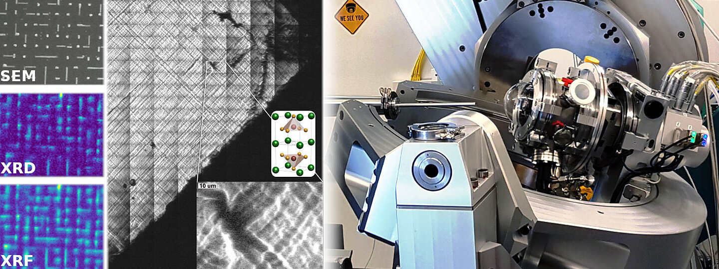
X-Ray Diffraction
Using state-of-the-art X-ray techniques, we aim to achieve a fundamental understanding of the correlation of structural and physical properties in crystalline materials. These investigations will also contribute to improving material perfection and pointing out paths for possible technological applications. For this purpose, we have a number of highly specialized instruments at our disposal at IKZ, including sophisticated experiments at synchrotron radiation sources.
Besides the determination of crystal orientation and crystal phases, we are primarily concerned with the elucidation of the real structure in bulk crystals and epitaxial layer systems. For ferroelectric thin films, we aim at a fundamental understanding of phase and domain formation, whereby phase transformations are identified and characterized by complex in situ experiments. For the verification of real structure models, corresponding simulations are developed.
Martin Schmidbauer, Albert Kwasniewski, Jutta Schwarzkopf
High-Precision Absolute Lattice Parameter Determination of SrTiO3, DyScO3 and NdGaO3 Single Crystals
Acta Cryst. B 68, 8-14 (2012)
DOI: 10.1107/S0108768111046738
Martin Schmidbauer, Dorothee Braun, Toni Markurt, Michael Hanke, Jutta Schwarzkopf
Strain Engineering of Monoclinic Domains in K0.9Na0.1NbO3 Epitaxial Layers: A Pathway to Enhanced Piezoelectric Properties
Nanotechnology 28, 24LT02 (2017)
DOI: 10.1088/1361-6528/aa715a
Laura Bogula, Leonard von Helden, Carsten Richter, Michael Hanke, Jutta Schwarzkopf, Martin Schmidbauer
Ferroelectric Phase Transitions in Multi-Domain K0.9Na0.1NbO3 Strained Thin Films
Nano Futures 4, 035005 (2020)
DOI: 10.1088/2399-1984/ab9f18
![[Translate to English:]](/fileadmin/user_upload/Forschung_Lehre/Abteilung_Materialwissenschaften/Sektion_Experimentelle_Charakterisierung/T_Roentgen_01.jpg "[Translate to English:]")
X-ray diffraction patterns of strained ferroelectric (K,Na)NbO₃ layers

In Situ TEM
Establishing the dynamic process-structure-function relationships under realistic conditions at relevant length and time scales are essential for achieving groundbreaking advancements in material science.
The In Situ TEM Group is committed to advancing materials science by visualizing, understanding, and controlling correlated chemical, structural, and electronic changes from the micro to atomic scale using in situ and operando TEM techniques. FAIR principles and AI will be implemented to streamline the workflows, standardize the procedures and enhance knowledge sharing among scientists.
Ultimately, we aim to expedite scientific discovery and drive innovation in materials science, positioning us in the forefront of the field.
We are committed to advancing the understanding and development of the electronic and photonic materials at IKZ and of our collaborative partners, leveraging through the power of in situ TEM techniques. Our research focuses on analyzing the fundamental aspects of phase transformation in oxides and uncovering the dynamics that govern the behavior of memristive materials for neuromorphic computing, LEDs, SiGe-based qubits for quantum computing under operational conditions. To achieve this, we employ a suit of cutting-edge TEM techniques, including HRTEM, HAADF, DPC, iDPC, EDS, EELS, 4DSTEM. Complemented by MEMS-based in situ TEM platforms, in situ TEM allows us to delve into dynamic changes of elemental distribution, strain, polarization, bandgap, electric field and other relevant parameters down to the atomic scale. Simultaneously, the electric or optical properties will be measured in a parallel fashion.
In addition to material studies; we also engage in methodological innovations, including advanced FIB sample preparation techniques, on chip calorimetry, correlative data analysis among others. To ensure the integrity of our findings, we rigorously assess potential non intrinsic modifications to the materials, such as those induced by electron beam irradiation, as well as any discrepancies between TEM sample and operational device geometry. This comprehensive approach aims to provide a thorough understanding of the underlying mechanisms spanning from fundamental research to industry-level material development initiatives.
![[Translate to English:]](/fileadmin/_processed_/7/0/csm_T_in-situTEM_36eca7334a.jpg "[Translate to English:]")
Schematic illustration of in situ TEM with AI powered workflow, including instrument control, data acquisition and data analysis. Dan Zhou et al. Next Materials 1(2023), 100007

Junior Research Group "All-GO-HEMT"
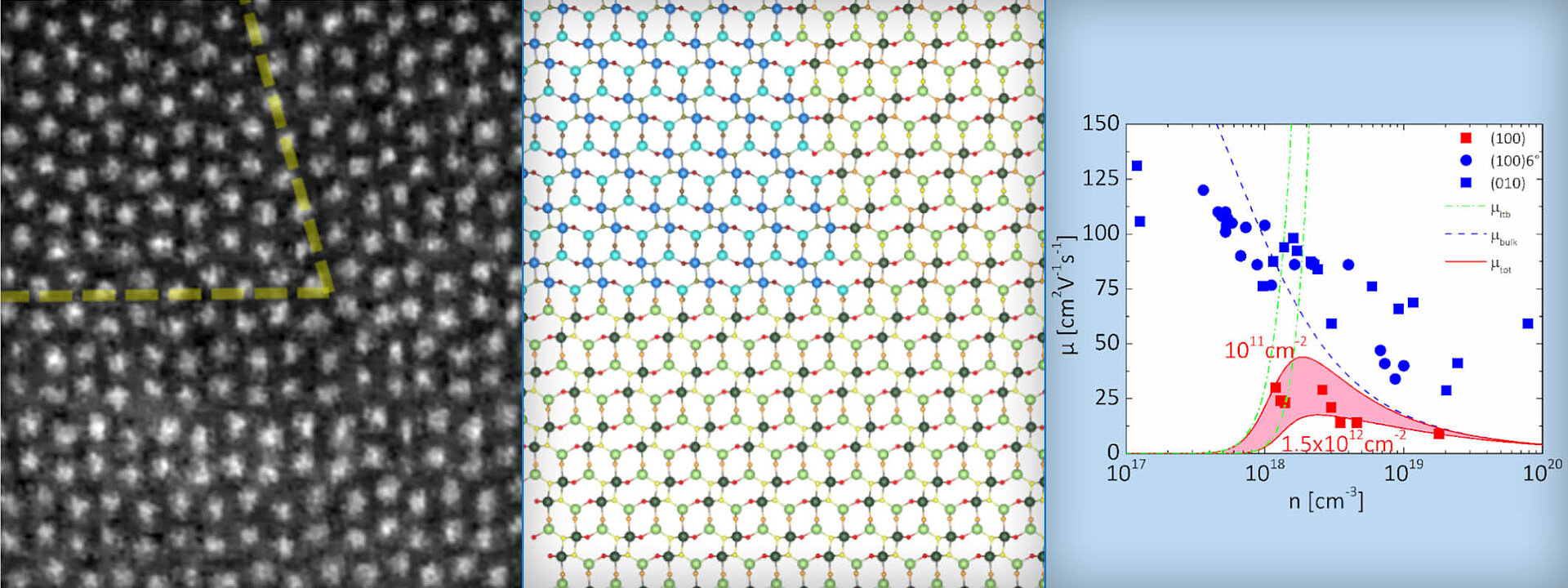
Semiconductor-based power electronics is a key technology for solving one of the greatest challenges facing society - sustainable energy generation/energy conversion. In addition to the conversion of energy generation to renewable and decentralized sources, the efficient use of energy is the most important lever for achieving sustainability goals in the energy sector. More efficient power electronics not only help to reduce harmful emissions through more efficient use of energy, but also increase the economic efficiency of energy-intensive processes. The “All-GO-HEMT” project therefore aims to significantly increase efficiency in power electronics by developing β-(AlxGa1-x)2O3/Ga2O3 heterostructures with high electron mobility. Under the lead of Dr. Andreas Fiedler, the All-GO-HEMT (03XP0630) project, funded by the Federal Ministry of Research, Technology and Space (BMFTR) as part of the NanoMatFutur program for young scientists, is laying an essential foundation stone in the field of science for technology sovereignty.
A high degree of interdisciplinarity is essential for the implementation of the research project. All-GO-HEMT achieves this by interlinking the expertise of the IKZ work areas of electrical characterization, epitaxy and electron microscopy. Specifically, the project aims to develop the first β-(AlxGa1-x)2O3/Ga2O3 heteroepitaxy process using MOVPE (metal organic vapor phase epitaxy) with homogeneous layer thickness, smooth interface, high aluminum content and delta doping over the entire substrate size of up to 2 inches.
The structural properties of the epitaxial layers are investigated using state-of-the-art electron microscopy methods, which enable the correlation of atomic structure mapping with atomic chemical mapping, the analysis of the electronic structure and electric field profiles. The evaluation of the material for use in power electronics is carried out by characterizing the electrical properties. Current transport and capacitive measurements are used to determine important electrical characteristics of the structures as a function of the growth conditions, such as the free charge carrier concentration and mobility, the concentrations of dopants and compensating defects. Our experience shows that the electrical properties characterize the perfection of the layer very sensitively. Fast feedback between electrical measurements and epitaxy is essential to optimize the material quality.
The precise adjustment of electrical conductivity is also necessary for other semiconductor crystals which are used in the device technology of modern electronics. Therefore, our characterization methods for determining the electrical properties, such as conductivity and Hall effect measurements (50 mK - 1100 K), deep-level transient spectroscopy (DLTS) (20 K - 800 K) and photothermal ionization spectroscopy as well as contact preparation are continuously adapted and expanded to meet the different requirements of the various semiconductor crystals, e.g. through additional photoexcitation.
Furthermore, the junior research group focuses on the technology transfer in close collaboration with industry partners in order to make scientific achievements accessible to society.
Andreas Fiedler, Robert Schewski, Michele Baldini, Zbigniew Galazka, Günter Wagner, Martin Albrecht, Klaus Irmscher
Influence of incoherent twin boundaries on the electrical properties of β-Ga2O3 layers homoepitaxially grown by metal-organic vapor phase epitaxy
J. Appl. Phys. 122, 165701 (2017).
DOI: 10.1063/1.4993748
Andreas Fiedler, Robert Schewski, Zbigniew Galazka, Klaus Irmscher
Static dielectric constant of β-Ga2O3 perpendicular to the principal planes (100),(010), and (001)
ECS Journal of Solid State Science and Technology, 8 (7) Q3083-Q3085 (2019).
DOI: 10.1149/2.0201907jss
Palvan Seyidov, Joel B Varley, Ymir Kalmann Frodason, Detlef Klimm, Lasse Vines, Zbigniew Galazka, Ta‐Shun Chou, Andreas Popp, Klaus Irmscher, Andreas Fiedler
Thermal Stability of Schottky Contacts and Rearrangement of Defects in β-Ga2O3 Crystals
Adv. Electron. Mater. 11, 2300428, (2025).
DOI: 10.1002/aelm.202300428
Schematic diagram showing the implementation of the β-(AlₓGa₁₋ₓ)₂O₃/Ga₂O₃-heterostructures planned in the “All-GO-HEMT” project.

Optical Spectroscopy
Our mission is to gather a detailed understanding of fundamental physical properties of bulk crystals and thin films. In this context, optical spectroscopy represents a highly versatile analytical characterization tool. We focus on the investigation of optical processes, which hold information about material-specific properties. This includes intrinsic characteristics of the system, such as band gaps or vibronic states, as well as extrinsic properties related to structural- or point defects. We are conducting research on novel crystal systems that have been grown in-house, as well as those supplied from collaborating partners.
Currently, the materials under investigation comprise novel oxides for memristive applications, as well as III-Nitrides for optoelectronics. To study their physical properties, we have a variety of experimental methods at our disposal. Next to widely used techniques such as emission-, absorption-, Raman spectroscopy, we also perform high spatial resolution cathodoluminescence spectroscopy. In addition, self-developed systems offer the possibility of measuring parameters which are experimentally difficult to access. This includes transmission spectroscopy of volume crystals at very high temperatures > 1000°C for studying the temperature dependence of bandgaps or defect absorption bands. Moreover, for detecting inhomogeneities in large volume crystals, we apply 3D tomographic analysis of scattered light.
![[Translate to English:]](/fileadmin/_processed_/1/6/csm_T_OptSpektr_22_9411821c52.jpg "[Translate to English:]")
Fig (a) Spatially resolved cathodoluminescence of an AlGaN layer revealing local distortions of step flow growth due to step pinning. (b) Sketch of the step pinning resulting in curved surface steps and local step bunching. (c) Infrared absorption spectra of the local vibrational modes of the tri-carbon defect in GaN crystals with different ¹²C/¹³C isotope contents and derived atomic arrangement.
