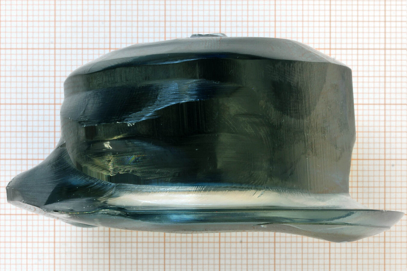
The obtained crystals have a usable length of up to one inch revealed and a high structural quality characterized by narrow X-ray rocking curves. Due to the Si doping the material is n-type conductive. Important for high-power applications, the electrical properties are not affected by a heat treatment at temperatures up to 1000°C even in an oxidizing atmosphere. Both high structural quality and electrical properties make the crystals well suited as substrates for homoepitaxy and fabrication of efficient power electronic devices in a vertical configuration.
[1]
Z. Galazka, S. Ganschow, K. Irmscher, P. Seyidov, M. Pietsch, T.-S. Chou, S. Bin Anooz, R. Grueneberg, A. Popp, A. Dittmar, A. Kwasniewski, M. Suendermann, D. Klimm, T. Straubinger, T. Schroeder, M. Bickermann
2 Inch Diameter, Highly Conducting Bulk β-Ga2O3 Single Crystals Grown by the Czochralski Method for High Power Switching Devices
Appl. Phys. Lett. 120 (2022) 152101
DOI:10.1063/5.0086996