Within the BMBF-funded consortium Advanced UV for Life, the IKZ develops processes for the production of AlN crystals and substrates as a basis for the manufacture of light-emitting diodes with ultra-short wavelengths (UVC-LED). The aim is to epitaxially grow the aluminum-rich AlxGa1-xN layers, in which the UV radiation is generated, on AlN substrates in order to realize low losses typically caused by non-radiative recombination due to a small lattice mismatch and resulting low dislocation densities. For this purpose, an AlN layer is first grown, which determines the crystalline quality of the following AlxGa1-xN layers.
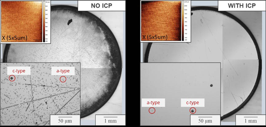
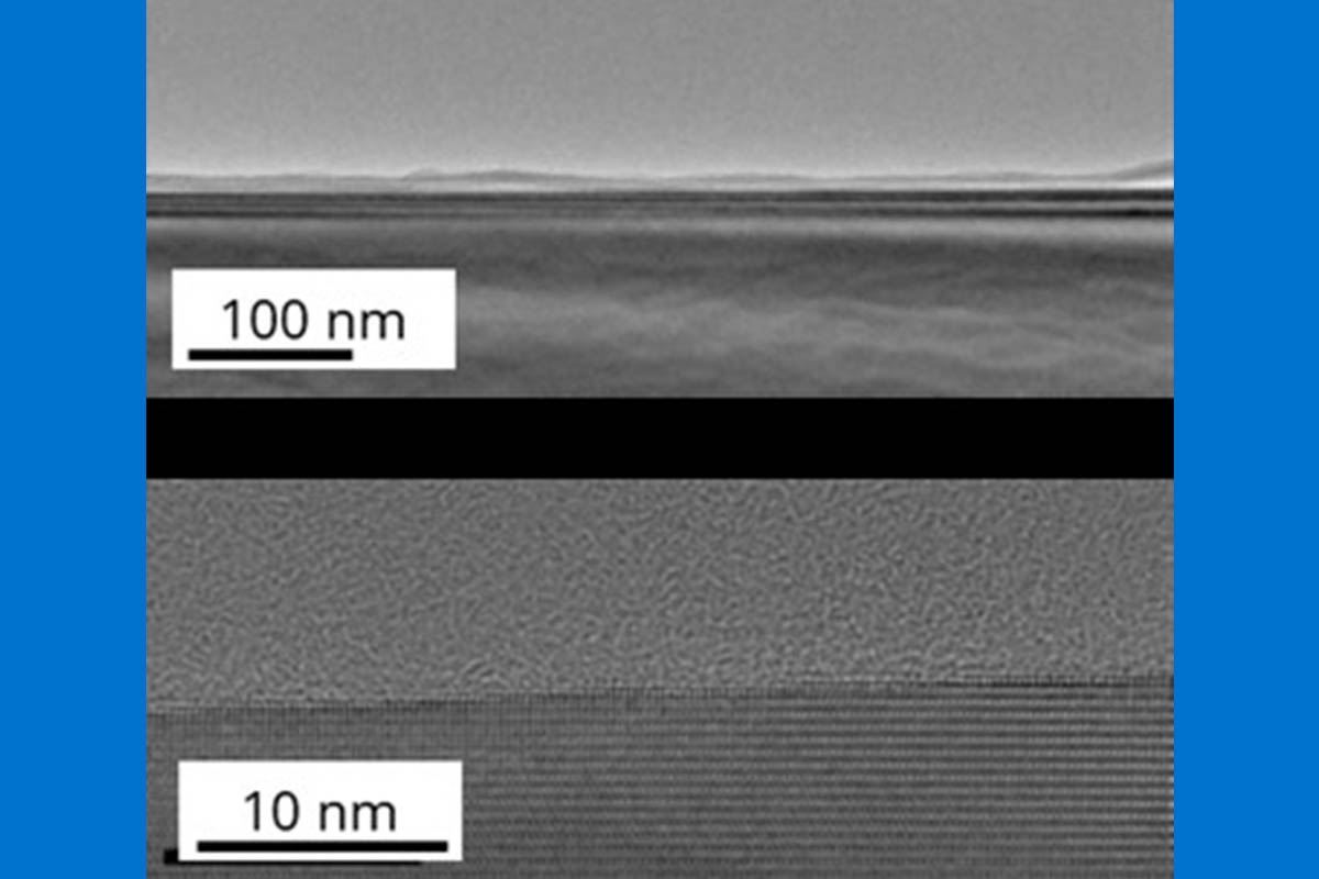
A prerequisite for the growth of defect-free epitaxial layers is not only a low dislocation density in the bulk crystals but also an exact and homogeneous orientation of the substrates over the entire wafer and the preparation of a defect-free surface by suitable polishing processes. The ideal orientation (0.2° tilted to the crystal axis) determined together with the project partners Ferdinand-Braun-Institut (FBH) and the group of Prof. Kneissl at the TU Berlin could be exactly adjusted by means of a processing and measuring technology developed together with the project partner CrysTec GmbH. After the use of a standard process for chemical-mechanical polishing (CMP), there are still defects under the surface which are no longer detectable with conventional surface characterization methods, but which generate typical linear dislocation accumulations in the AlN layers grown at the FBH by metal organic gas phase epitaxy (MOVPE) [Fig. 1: left]. The damage layer can be removed before epitaxy, e.g. by plasma etching (ICP) [Fig. 1: right]. By means of transmission electron microscopy (TEM) it could be proven that the damage layer can already be completely removed with a CMP process optimized at the IKZ [Fig. 2].
In any case, the low-defect AlN epitaxial layers on precisely oriented AlN substrates provide an ideal basis for research work on aluminum-rich AlxGa1-xN layers or UVC LEDs with ultra-short wavelengths.
Weitere Informationen:
Thomas Straubinger
Section: Crystals for Electronics