Cathodoluminescence, the emission of photons upon excitation by accelerated electrons has the advantage over optical methods that the band gap energy of the materials that is investigated is not limited by the limited availability of optical excitation sources in a specific wavelength range.
The Section „Experimental Characterization“ at IKZ studies the relation between structural and optical properties of semiconductors by means of cutting edge electron microscopy, including aberration corrected TEM and cathodoluminescence. The group made major contribution to the field of III-Nitrides in the past. To keep the high level of research and to offer new possibilities the institute made a major investment and purchased a latest generation scanning microscope combined with the newest generation cathodoluminescence spectrometer.
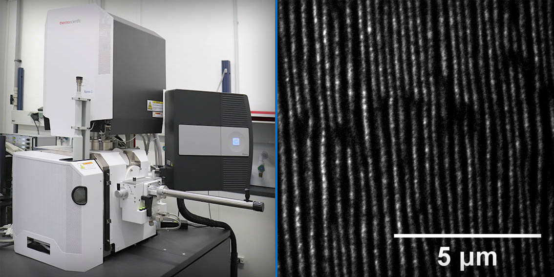
The new scanning electron microscope (Apreo S HiVac from Thermo Fisher Scientific) has a completely new lens design with three in-lens detectors that are highly versatile in obtaining complementary information with a resolution down to 0.7 nm. The completely new designed electron optics of the microscope combines an electrostatic lens and a magnetic dispersion lens that can be combined and appropriately tuned. This permits imaging even of insulating samples with high spatial resolution. The scanning transmission detector allows to study thin samples in transmission with a resolution of 0.8 nm. The microscope offers a wide range of emission currents up to 400 nA and is equipped with a He cooling stage.
The completely new designed Gatan Monarc CL spectrometer has a highly improved optical transmission, a high sensitivity in the deep UV range and a spectral resolution down to 0.1 nm. Three detectors, a CCD for parallel detection and photomultiplier for the ultraviolet and visible spectrum and a liquid nitrogen cooled wide range photomultiplier cover the wavelength range from 190 nm to 1.7 µm. Two exchangable mirrors with 10 mm and 5 mm focal length permit a wide field of view (10.000µm²) and a high spatial resolution (<10 nm) respectively.
With this new equipment at hand the section will focus on III-Nitrides in the deep UV and in the red spectral range. Fig. 1 a shows as an example a panchromatic image of a 20 nm (Al,Ga)N layer on a AlN substrate. Ga rich AlGaN islands are visible that align along the step edges of the offcut substrate. The image is taken at room temperature. Such images offer valuable insight into the growth process of such layers and help to optimize it with respect to getting improved deep UV emitters.
More Information:
Martin Albrecht
Section Experimental Characterization