One of the observatory’s greatest technological challenges
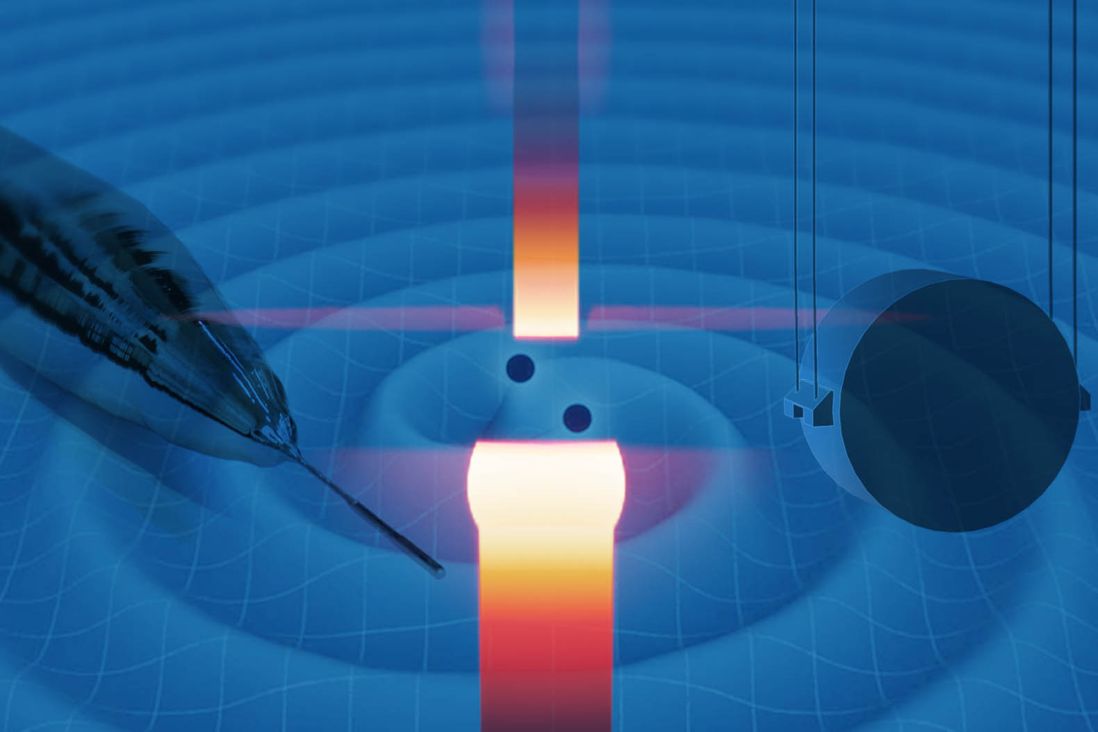
Among other components, the Einstein Telescope will include a dedicated low-frequency interferometer (ET-LF) that must operate at cryogenic temperatures of 10 to 20 K to minimize thermal noise. At the heart of this interferometer are large-format mirrors made of high-purity silicon. These substrates must combine extremely low optical absorption and excellent mechanical properties with dimensions that far exceed those currently feasible using established production processes. The system also requires sophisticated cryogenic suspension systems and stable ultra-high-vacuum conditions for uninterrupted long-term operation.
This is precisely where Project D comes in: the participating partners - including the German Center for Astrophysics (DZA), the Karlsruhe Institute of Technology (KIT), and OTH Regensburg - are pooling their expertise in crystal growth, materials science, and cryogenics to develop scalable solutions for the ET-LF mirrors.
The IKZ’s role
The IKZ is involved in two of the consortium’s seven subprojects. Under the direction of Dr. Iryna Buchovska, Project D3 systematically investigates the influence of impurities and process parameters on the optical, thermal, and mechanical properties of crystalline silicon. The focus is on the requirements for both mirror substrates and monocrystalline silicon fibers used in the suspension systems.
Project D4 investigates the Magnetic Czochralski (MCz) process as a promising method for producing large-diameter silicon crystals with the optical purity required for ET-LF. The process is combined with a “self-crucible” technique patented by the IKZ to prevent crucible contamination. This subproject is led by Priv.-Doz. Dr. habil. Radhakrishnan Sumathi.
The goal is to address a long-standing challenge: while the established float-zone process (FZ) already achieves the optical purity required for ET-LF, its maximum achievable diameter has remained at around 200 mm for decades - significantly below the required mirror size of more than 450 mm. The Czochralski (Cz) process, on the other hand, can produce silicon crystals with diameters of up to 450 mm. However, contact between the melt and the quartz crucible, together with the use of graphite heaters, leads to significantly higher impurity levels and, consequently, optical absorption that is approximately 100 times higher than in FZ silicon. No industrial process currently available therefore combines the required purity with the necessary diameter for silicon mirrors suitable for the Einstein Telescope. This is precisely where the IKZ’s research comes in.
Beyond basic research
The technologies developed in the project are relevant not only to the Einstein Telescope. High-purity silicon is also a key material for power electronic components supporting the energy transition, as well as for silicon-based quantum technologies. The project thus contributes to Germany’s High-Tech Agenda, particularly in the fields of microelectronics and quantum technologies, while strengthening collaboration with the German semiconductor industry, including Siltronic AG and PVA TePla.
The total budget for Joint Project D amounts to approximately €3.7 million, of which around €1.5 million is allocated to the IKZ. The results will feed directly into the international design work of the Einstein Telescope Collaboration and are intended to strengthen Germany’s contribution to realizing this European flagship project.
Contact:
Leibniz-Institut für Kristallzüchtung (IKZ)
PD Dr. habil. Radhakrishnan Sumathi
Section Semiconductor / Cz
Phone: +49 (0) 30 / 246 499 401
Email
Dr. Iryna Buchovska
Section Semiconductor / FZ
Phone: +49 (0) 30 / 246 499 406
Email
Further information:
Preparatory Program for the Einstein Telescope - Joint Project D: Mirror Technologies for ET-LF