The ultra-wide band gap semiconductor AlN, as well as its the ternary cousin AlGaN, has a number of attributes that make this material system a promising one for electronic and optoelectronic devices. Thanks to the very wide bandgap, it can be used to make LEDs that emit in the deep and far UVC. The largest markets for such devices, which span 220 nm to 280 nm, are the disinfection of drinking water, waste water treatment, and direct disinfection of indoor air. As well as these opportunities in deep-UV photonics, AlN-based devices are compelling candidates for next-generation high-frequency power-conversion. Already, AlN-based high-power transistors are outperforming those made from the two most common wide bandgap semiconductors, SiC and GaN.
At this year's International Conference on Nitride Semiconductors (ICNS-14, held from Nov. 12-17, 2023 in Fukuoka, Japan), the growing interest in AlN substrate-based technologies was clearly evident. A total of 21 presentations dealt with the growth of AlN crystals, substrate preparation as well as epitaxy and device development using native bulk AlN substrates. Substantial progress was made in every area compared to the previous year, reflecting the high level of dynamism and commitment of the scientists involved.
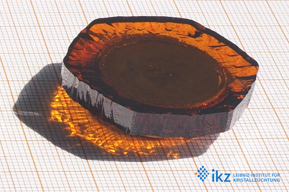
The IKZ AlN team was well represented by a recently published flyer and two presentations. Andrew Klump introduced a new AI-assisted tool for the quantification of impurities in AlN on his poster. Fast and non-destructive insights into the impurity concentrations can be achieved by UV absorption spectra calibrated with secondary ion mass spectrometry (SIMS) measurements. Carsten Hartmann showed a newly designed AlN growth process in his oral talk. The bulk AlN crystals reveal a very high crystalline quality combined with expansion angles of 45 degrees that can slash the time it takes to realise bulk AlN substrates with industrially relevant crystal diameters. The great interest in the presentations and the fruitful discussions with the international AlN players show the high esteem in which the work at the IKZ is held.
In the run-up to the ICNS the new AlN process was already published as an invited article in the Compound Semiconductor Magazine and as a scientific publication in the open access journal Applied Physics Express (APEX). The great interest is also evident here, with over 600 downloads of the APEX article so far.
The AlN team starts from the beginning of 2024 the supply of 1-inch substrates to scientific partners. 2-inch substrates will be demonstrated in the course of 2024.
Contact:
- Dr. Carsten Hartmann (IKZ) | E-Mail