Ferroelectric films are used for a variety of technological applications, such as non-volatile memory devices or ferroelectric field effect transistors (FeFETs). These applications exploit their property of exhibiting permanent electric polarization, which can be reversed by the application of an external electric field. The microscopic switching mechanism depends on the ferroelectric properties of the films, the structure and kinetics of the domains or domain walls, and the electrostatic boundary conditions. For example, by adding a dielectric film between the ferroelectric and the electrode with a thickness of only a few nanometers, a ferroelectric tunnel junction (FTJ) can be created, which could play a major role for "neuromorphic computing." On the other hand, the use of slightly thicker dielectric layers allows the exploitation of the negative capacitance (NC) effect and is interesting for ultra-low power devices. The ferroelectric properties as well as the domain formation in the layers, on the other hand, crucially depend on the structure and phase symmetry of the films. These can be specifically tuned by introducing a lattice strain in the layers ("strain engineering"). However, the underlying switching processes are not fully understood yet.
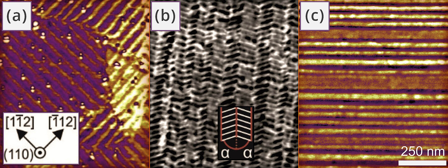
Therefore, within the DFG-funded project FeDiBiS (Polarization Switching Kinetics in Ferroelectric/Dielectric Bi-Layer Structures), the fundamental relationship between structural and electrical changes during the intentional switching of ferroelectric films will be investigated. For this purpose, lead-free ferroelectric potassium-sodium-niobate films are epitaxially deposited on oxide substrates grown in IKZ to adjust a targeted lattice strain in the films and thus selectively tune the ferroelectric polarization as well as the ferroelectric domains in the films. Metal-organic vapor phase epitaxy (MOVPE) is used to achieve the required high structural perfection in the films. The key advantage of this method is the epitaxial growth close to thermodynamic equilibrium, which allows the deposition of almost perfectly stoichiometric single crystalline films with a very regular domain pattern (see Fig.1). In addition to structural and electrical characterization of the films, operando studies of the films are planned. Using nanoprobe X-ray diffraction performed simultaneously with electrical measurements, this will shed light on the kinetics of polarization switching of the real device in a non-destructive way. These extremely demanding measurements are only possible at modern synchrotron radiation sources with focused X-rays in the range of 100 nanometers.
The project represents a joint project of the two sections "Thin Oxide Films" and "Experimental Characterization" of the IKZ as well as of NaMLab in Dresden and will start in May 2021. The work will also be performed within the framework of the ERDF (European Regional Development Fund) Application Laboratory "Materials for Oxide Electronics".
Further information:
Jutta Schwarzkopf
Section Thin Oxide Films


