![[Translate to English:]](/fileadmin/_processed_/e/4/csm_21_05_GaO_22_32637e9f90.jpg)
Crystalline gallium oxide is a promising substrate material for the production of next-generation power electronics devices (in particularly needed for the energy revolution). So far, gallium oxide crystals grown at the IKZ using the Czochralski process (CZ) have been used exclusively to produce substrates with (100) and (001) orientations, which can be cleaved along these easy cleavage planes and then polished also with off-orientation. However, since CZ-Ga2O3 crystals are grown along the (010) direction and have a slightly elliptical shape, 2" diameter substrates can be efficiently prepared from crystals parallel to the (010) plane only. To evaluate the suitability of (010) substrates for epitaxy and device fabrication, crystals with a diameter of 20 mm were grown at the IKZ, processed into 5x5 mm² (010) substrates and successfully overgrown with gallium oxide epitaxial layers using MOCVD. The main challenge was to cut the crystals perpendicular to the cleavage planes without cracks and to polish them without chipping.
The IKZ has many years of experience in growing Ga2O3 single crystals using the Czochralski method and in producing homoepitaxial layers, in particular on Mg-doped (100)-oriented Ga2O3 substrates with a defined off-orientation, which are usually produced from IKZ crystals by the Berlin industrial partner CrysTec GmbH. For these substrates, epitaxial growth conditions yielding step flow have been developed at the IKZ and, among other things, layers with world record high mobility values of 153 cm-2 Vs-1 at a charge carrier concentration of 1.4 x 1017 cm-3 were demonstrated.
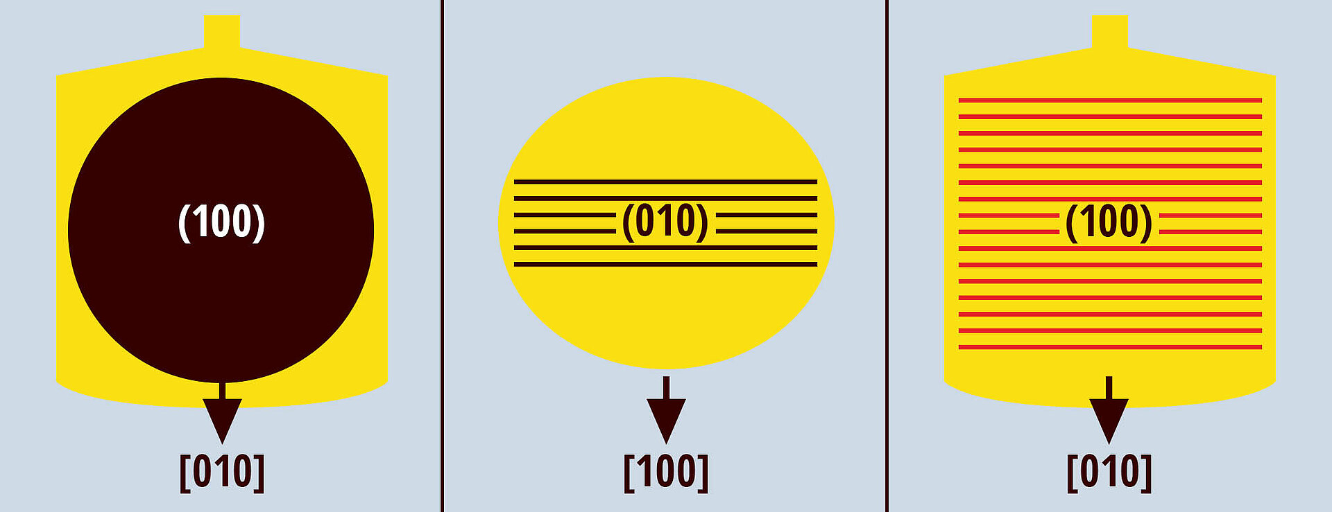
Fig. 1 schematically shows the preparation of 2" substrates from a typical CZ-grown crystal with a slightly elliptical shape and a minimum diameter of 2". Wafers with (010) orientation can be prepared with comparatively low material loss, but only a few wafers with (100) orientation. The preparation of (010) substrates therefore seems to be more economical at first glance. Anyway, decisive for the choice of substrate orientation is not only the substrate price but also whether high-quality epitaxial layers can be produced on the substrates or what device performance can be achieved. Here, too, the race is still open. Step flow has already been demonstrated for epitaxial layers grown on substrates with (100) orientation, but although layers grown on (010)-substrates typically show no step flow but a facetted surface, also good layer properties can be realized on them. Additionally, step flow growth on (100) substrates is only stable in a comparatively small process window.
For the production of (010) substrates at IKZ, Mg-doped crystals with a diameter of approx. 20 mm and a length of approx. 50 mm grown in the (010) direction by the CZ-method at IKZ were used. Due to the easy cleavage of the material gallium oxide along the (100) and (001) planes, cracks easily occur along the cleavage planes when cutting the crystals parallel to the (010) plane using standard processes (Fig. 2 - top left) and could only be avoided by embedding the crystals and using a special sawing technology (Fig. 2 - bottom left). As the substrates also tend to form chipping marks at the edges during polishing (Fig. 2 - top centre), they were protected by an embedding technology developed at the IKZ. This way, substrates with 5 mm and 10 mm edge length could be produced without edge chipping (Fig. 2 - bottom centre). Finally, material-specific chemical mechanical polishing processes were developed and optimized at the IKZ to produce surfaces without micro-scratches (Fig. 2 - right).
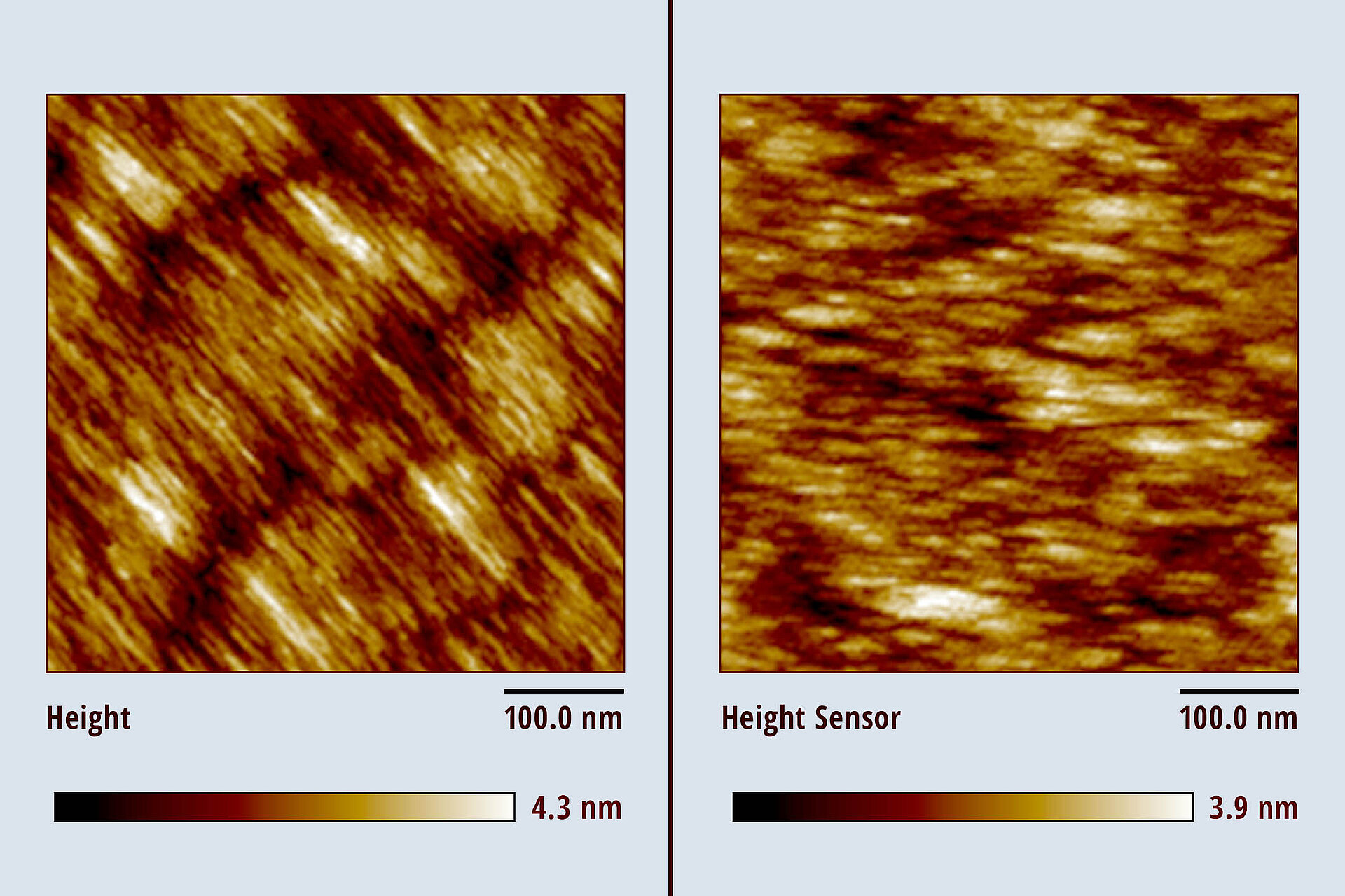
The gallium oxide substrates with on-axis (010) orientation were homoepitaxially overgrown at the IKZ with an approx. 300 nm thick gallium oxide layer using MOCVD and standard process conditions at a comparatively high growth rate of approx. 820 nm/h. The epilayer surface (Fig. 3 - left) shows a facetted morphology with the appearance of elongated features oriented along the [001] direction which is comparable to surfaces obtained at the IKZ (Fig. 3 - right) and at other research groups [9] on commercially available (010)-substrates from Tamura Inc.
The properties of the grown layers will now be investigated in detail, and machining and epitaxy processes will be subsequently optimized. In addition, the influence of the substrate misorientation on the layer properties will be evaluated.
This work was performed in the framework of the Leibniz-Science Campus GraFOx. The work was funded in part by the Bundesministerium für Bildung und Forschung (BMBF) under grant numbers 03VP03712 and 16ES1084K and the European Regional Development Fund (ERDF) of the European Commission under grant number 1.8/15.
Further information:
Thomas Straubinger
Section Crystalline Materials for Electronics