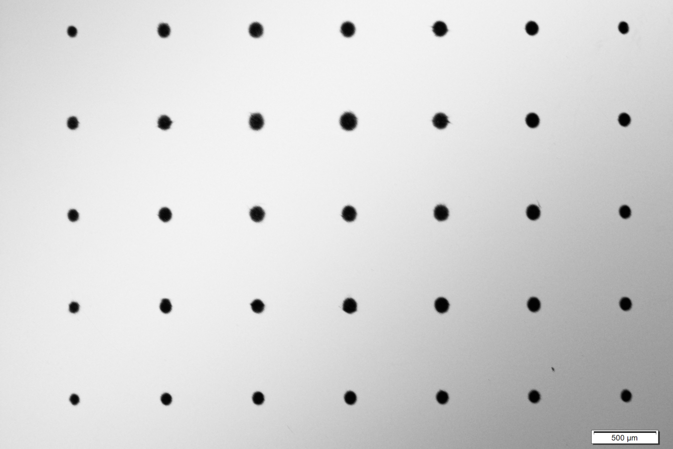
The approach of using laser radiation to grow patterned crystalline structures on amorphous surfaces, thereby replacing complex masks or lithography techniques, has been successfully realized.
For this purpose, laser radiation with a specific wavelength and intensity was employed and directed through a diffractive optical element (DOE), creating a patterned thermal inhomogeneity on the target substrate.
Thermal decomposition of organometallic gases at elevated temperatures was used to selectively form liquid and, subsequently crystalline island-shaped structures on the surface. Using this method, CuInSe2 islands in the micrometer range were fabricated and processed into micro-concentrator solar cells.
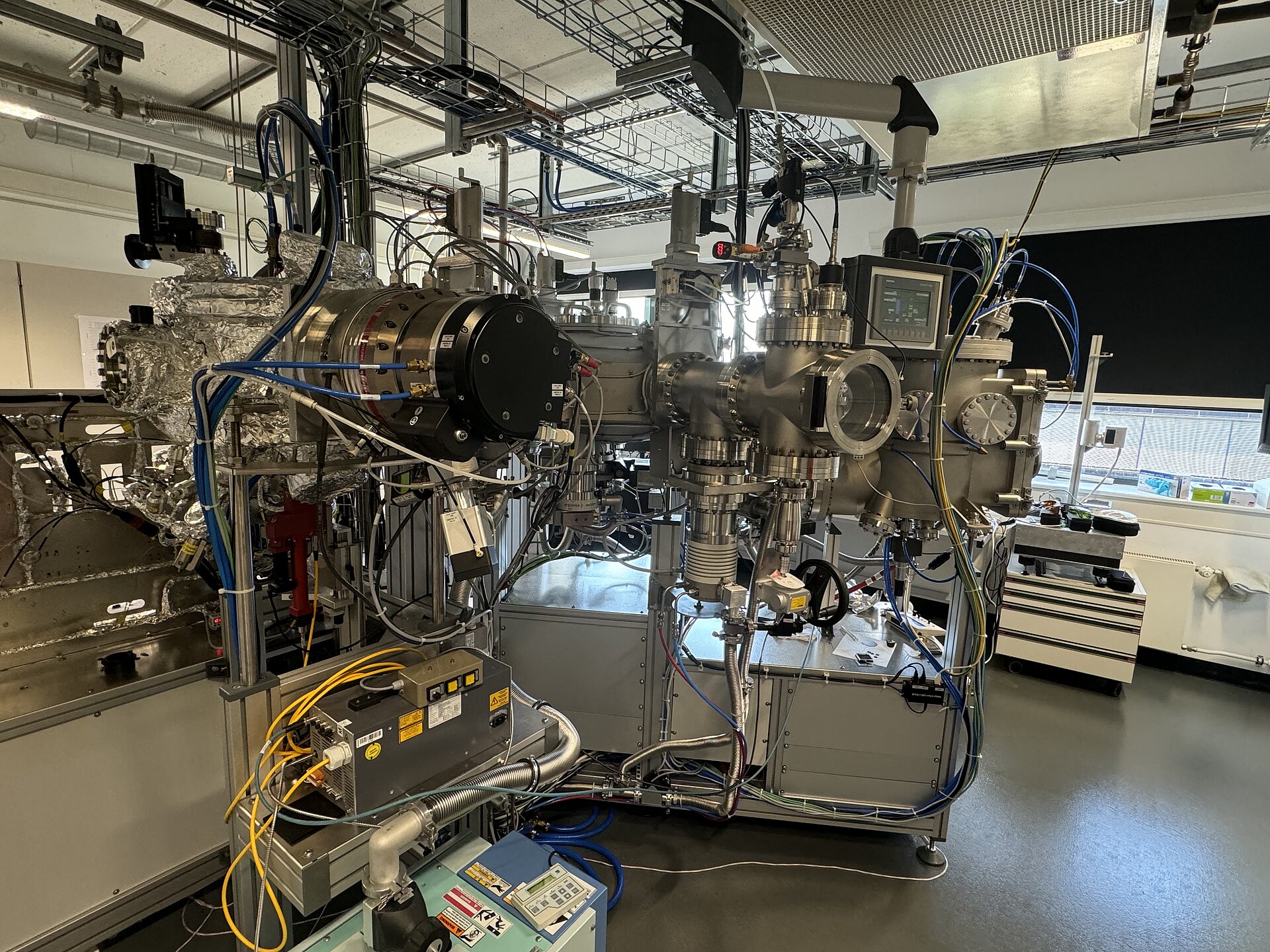
For this project, a PVD-CVD cluster system (physical vapor deposition and chemical vapor deposition) with an integrated laser system has been developed and tested. The locally selective deposition of the localized structures in the micrometer range can be used for a variety of other applications, particularly in semiconductor industry.
The project partners IKZ, BAM, UDE and the company BESTEC, as well as the contractors Mergenthaler GmbH, CSE GmbH and the Fraunhofer Heinrich Hertz Institute Berlin worked closely together to realize the project.
Kontakt:
Leibniz-Institut für Kristallzüchtung (IKZ)
Dr. Setareh Zahedi-Azad
Tel.: +49 30 6392-2852
Email:setareh.zahedi-azadikz-berlin.de
Dr. Torsten Boeck
Tel.: +49 30 6392-3051
Email:torsten-boeckikz-berlin.de


