These oxides are grown as thin layers with thicknesses ranging from 10 nm to 5 µm and act as the electrically active part of the component. Areas of application for such oxide components include non-volatile memory devices, sensors, microactuators or transistors for power electronics. Oxide structures of highest material quality and the understanding of their physical properties are essential prerequisites for the technological mastery of metal oxides for technological applications.
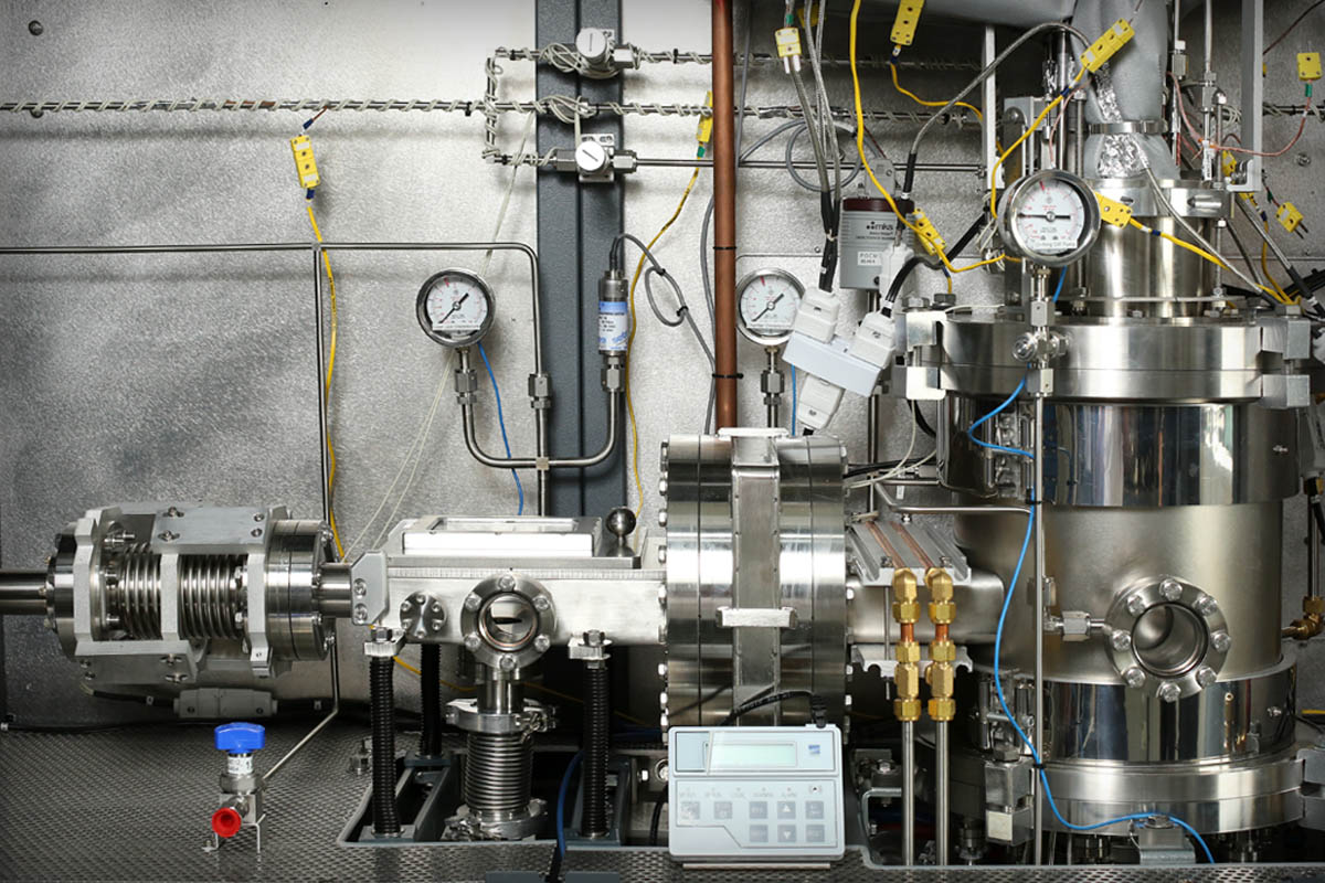
Since March 2017, the ERDF (European Regional Development Fund) application laboratory "Materials for Oxide Electronics" has been pursuing the goal of developing oxide functional layers with high structural perfection for application-relevant component test structures and making them available to industrial partners. The deposition of single-crystalline, low-defect oxide layers with defined electrical and structural properties adapted by doping and strain engineering forms the basis for this. In order to achieve the high structural perfection of the layers, the method of metal-organic vapor phase epitaxy (MOVPE) is used, which is already the deposition method of choice in industry due to its scaling potential. Within the ERDF-project a new MOVPE system was purchased with subsidies to expand the material base. The new system has now been installed and commissioned in the "Thin Oxide Films" section of the IKZ. In the first phase binary niobium oxide layers were deposited as a test system. In the second stage ferroelectric sodium-niobate layers are grown. Here the parameter range for single crystalline, stoichiometric layers has to be tested. First tests have been successfully carried out. In the next months it is planned to expand the material base to potassium-sodium-niobate layers with different strain states. For this purpose, mainly rare-earth scandate crystals from the IKZ are used as substrates. In cooperation with project partners, these layers are planned to be used both for memory components and for SAW sensors.
Also by using MOVPE, homoepitaxial β-Ga2O3 layers are deposited on in-house grown substrates in the section "Thin Oxide Films". In order to exploit the promising properties of the material, such as the high electric breakdown field strength, even more efficiently, work is currently being carried out on layer structures for vertical power devices. If the industrial relevance of β-Ga2O3 can be demonstrated, the material system has a high potential to become the next high-performance material for power electronics, beyond SiC and GaN.
In close cooperation with the section "Experimental Characterization" the oxide layers are characterized with respect to their electrical and structural properties. Equipment procured from ERDF funds are also used for this purpose.
To conclude the ERDF project, a workshop is planned for September 22th, 2020 for the official opening of the application laboratory with lectures on power devices based on gallium oxide layers and thin-film sensors based surface acoustic waves. The workshop is aimed at representatives from universities, non-university institutes and industry.
More Information:
Jutta Schwarzkopf
Section Thin Oxide Films