β-Ga₂O₃ is considered one of the most promising materials worldwide for future energy-efficient power electronics. With its ultra-wide bandgap of approximately 4.8 eV, the material enables theoretical breakdown field strengths of up to 8 MV/cm and could therefore significantly outperform established technologies based on silicon carbide (SiC) or gallium nitride (GaN). Another major advantage is the possibility of producing large-volume single crystals from the melt at comparatively low cost. However, the scientific community has not yet reached a clear consensus regarding the optimum surface orientation for lateral power devices. This is mainly due to the lack of direct comparative studies on devices fabricated on different crystal orientations.
The objective of the project is therefore to answer the still open question of the optimal crystal orientation for high-performance β-Ga₂O₃ transistors. The focus lies on the two most technologically relevant surface orientations, (100) and (010). Due to the anisotropic crystal structure of β-Ga₂O₃, both orientations exhibit different electrical, thermal, and structural properties, which strongly influence the quality of epitaxial layers and ultimately the performance of the devices.
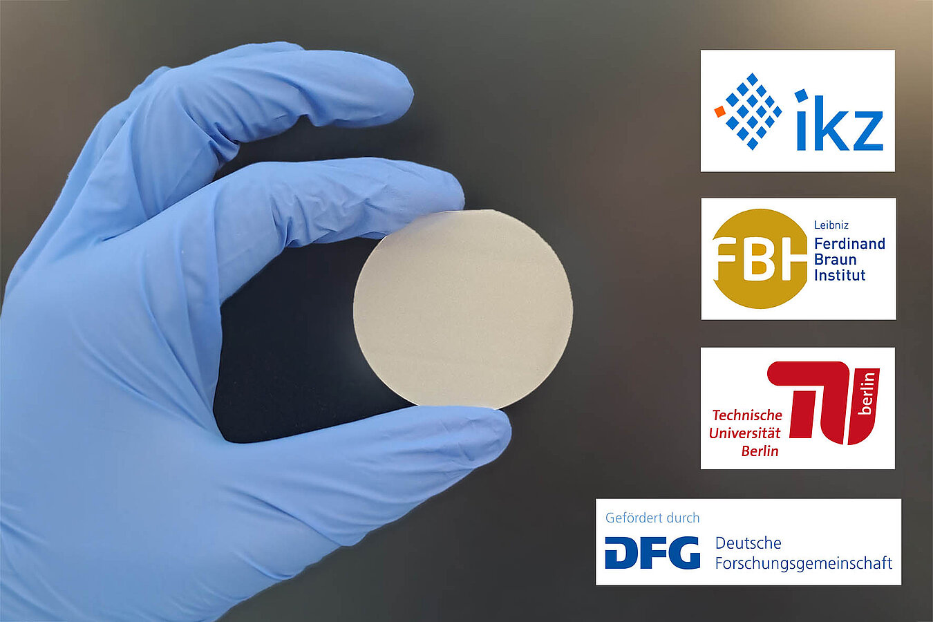
The IKZ contributes its internationally recognized expertise in the growth of β-Ga₂O₃ single crystals and the homoepitaxial MOVPE deposition of high-quality thin films. Already today, electron mobilities exceeding 160 cm²/(Vs) at very low doping concentrations have been achieved at IKZ on (100)-oriented substrates - values that rank among the best reported worldwide. In addition, the institute is working on scaling to larger wafer formats up to 2-inch substrates.
Based on the epitaxial structures fabricated at IKZ, the Ferdinand-Braun-Institut develops high-performance lateral high-voltage transistors. Previous work has already demonstrated breakdown voltages up to 1.8 kV and record power densities of 155 MW/cm². Within the new project, devices with blocking voltages of 1500 V and pulse currents up to 20 A are targeted to demonstrate β-Ga₂O₃-based real high-performance transistors for the first time. At the same time, novel concepts for suppressing leakage currents and improving interface quality will be developed in order to push the devices closer to the theoretical material limits.
The Technische Universität Berlin complements the project with extensive expertise in the dynamic characterization of power transistors under realistic switching conditions. Particular focus will be placed on switching losses, reliability, and thermal stability. In the long term, the project aims to realize a demonstrator for future energy-efficient power electronics.
The project therefore covers the complete development chain - from crystal growth and wafer processing to epitaxy, device fabrication, and system integration. The researchers expect to gain fundamental insights into how material properties, crystal orientation, and interface characteristics affect the performance of future gallium-oxide high-power transistors. In this way, β-Ga₂O₃ could make a decisive contribution to more compact, efficient, and powerful next-generation power conversion systems.
Contact
Leibniz-Institut für Kristallzüchtung (IKZ)
Dr. Andreas Popp
Phone: +49 (0) 30 / 246 499 312
Email
Dr. Zbigniew Galazka
Phone: +49 (0) 30 / 246 499 416
Email