Section Thin Oxide Films
Section Thin Oxide Films
Mission
Oxide layers can be used as the electrically active part of a device offering new application prospects compared to bulk crystals and ceramics. By utilizing dopants or lattice strain, their functional properties can be specifically adapted to desired requirements. Smaller device structures in epitaxial thin layers not only provide less material consumption, but also allow improved device parameters such as higher processor speed or higher operation frequencies for filters or sensors. In addition, using remote epitaxy or sacrificial layers, free-standing oxide films and novel oxide heterostructures can be fabricated, which are not possible by conventional methods due to incompatibility of growth conditions, e.g. different lattice parameters or symmetries. Our mission is to develop single-crystal oxide films with optimized properties tailored to the application.
Research activities
The main focus of our work is the development of oxide thin films with tailored semiconducting, dielectric or ferro/piezoelectric properties. The deposition methods available at IKZ are metal-organic vapor phase epitaxy (MOVPE) and pulsed laser deposition (PLD). Our activities include oxide films with thicknesses between a few nanometers and several micrometers with large potential for application in high-power electronics, ferroelectric memory devices, piezoelectric sensors and energy harvesters.
Head of section

Topics
Strained functional perovskite films
Functional oxide films with perovskite structure exhibit a variety of functional properties depending on their chemical composition and structure. In contrast to bulk crystals, in epitaxial layers additional degrees of freedom are given by incorporating lattice strain (strain engineering by heteroepitaxy) or intentional defects (defect engineering) to deliberately modify material properties and to develop new technologies. Our mission is to make promising materials with perovskite structure, such as the lead-free ferro/piezoelectric material Potassium-Sodium-Niobate ((K,Na)NbO3) or the dielectric Strontium-Titanate (SrTiO3), available in thin film form for potential applications, e.g. for highly sensitive sensors, electro-optical modulators or neuromorphic computing.
In close collaboration with the sections "Oxides & Fluorides" and "Experimental Characterization", we grow (K,Na)NbO3 and SrTiO3 based films using the metal-organic vapor phase epitaxy (MOVPE) method as the only group worldwide. By introducing lattice strain or the intentional deviation from nominal stoichiometry, material properties (such as piezoelectric constants, phase transition temperature, dielectric permittivity) are deliberately modified. Film characterization using scanning probe microscopy techniques such as piezoelectric force microscopy (PFM) and conductive atomic force microscopy (CAFM), provides insight into ferroelectric domain formation and electrical properties at the nanometer scale.
Mohamed Abdeldayem, Chang-Ming Liu, Izaz-Ali Shah, Andreas Fiedler, Detlef Klimm, Martin Albrecht, Jutta Schwarzkopf
Epitaxial Growth of CaTiO3 Thin Films by Metal Organic Vapor Phase Epitaxy for Potential Applications in Memristive Devices
Cryst. Growth Des. 25, 3654 (2025)
DOI: 10.1021/acs.cgd.4c01412
Sijia Liang, Dennis Finck, Marc W. Neis, Jutta Schwarzkopf, Dirk Mayer, Roger Wördenweber
SAW gas sensor based on extremely thin strain-engineered K0.7Na0.3NbO3 films
Appl. Phys. Lett. 119, 112905 (2021)
DOI: 10.1063/5.0060796
Yankun Wang, Saud Bin Anooz, Gang Niu, Jinyan Zhao, Martin Schmidbauer, Lingyan Wang, Wei Ren, and Jutta Schwarzkopf
Evolution of domain structure in epitaxial ferroelectric K0.5Na0.5NbO3 films grown by metal-organic vapor-phase epitaxy
Phys. Rev. Mater. 8, 054409 (2024)
DOI: 10.1103/PhysRevMaterials.8.054409
Liyan Dai, Jinyan Zhao, Jingrui Li, Bohan Chen, Shijie Zhai, Zhongying Xue, Zengfeng Di, Boyuan Feng, Yanxiao Sun, Yunyun Luo, Ming Ma, Jie Zhang, Sunan Ding, Libo Zhao, Zhuangde Jiang, Wenbo Luo, Yi Quan, Jutta Schwarzkopf, Thomas Schroeder, Zuo-Guang Ye, Ya-Hong Xie, Wei Ren & Gang Niu
Highly heterogeneous epitaxy of flexoelectric BaTiO3-δ membrane on Ge
Nature Communications 13, 2990 (2022)
DOI: 10.1038/s41467-022-30724-7
![[Translate to English:] [Translate to English:]](/fileadmin/_processed_/a/5/csm_T_versp_Oxidsch_398d5e0304.jpg)
Schematic presentation of the influence of tensile (left) and compressive (right) strain on a perovskite unit cell and the polarization P

Sacrificial layers and free-standing oxide films
Alternatively, to strain engineering by heteroepitaxial film growth on lattice mismatched substrates, local lattice strain and strain gradients on the nanometer scale can be generated by the formation of artificial twist boundaries or externally applied mechanical stresses in thin oxide films. This is achieved by transferring and bonding a free-standing ultrathin oxide film on a single-crystal substrate with a controlled twist-angle or stacking free-standing oxide layers on a foreign substrate. Our aim is to investigate the effects of the resulting dislocation network on the dielectric and ferroelectric properties of thin complex oxides and to tune the functional properties by external strain.
In order to achieve free-standing nanometer-thin oxide layers, the concept of the sacrificial layer, produced using pulsed laser deposition (PLD) technology, and the overgrowth of the functional oxide layer by PLD or MOVPE is applied. The layer transfer is carried out with our newly developed layer transfer station, which operates under high vacuum conditions (see section “Nanostructures”). We apply different X-ray methods (see “Experimental Characterization”) and scanning probe techniques to gain fundamental insights into defect and domain formation after subsequent bonding on a new substrate or after applying an external stress.
Martin Schmidbauer, Jeremy Maltitz, Ferris Stümpel, M. Hanke, Carsten Richter, Jutta Schwarzkopf, and Jens Martin
Periodic lateral superlattice in bonded SrTiO3/SrTiO3 twisted Perovskites
Appl. Phys. Lett. 126, 101902 (2025)
DOI: 10.1063/5.0251478
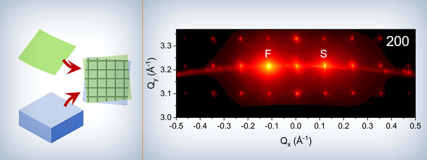
Left: Schematics of the fabrication of artificial twist boundaries | Right: Signature of a periodic screw displacement network at the interface of a twisted SrTiO₃ membrane on an SrTiO₃ substrate produced by a transfer bonding process
