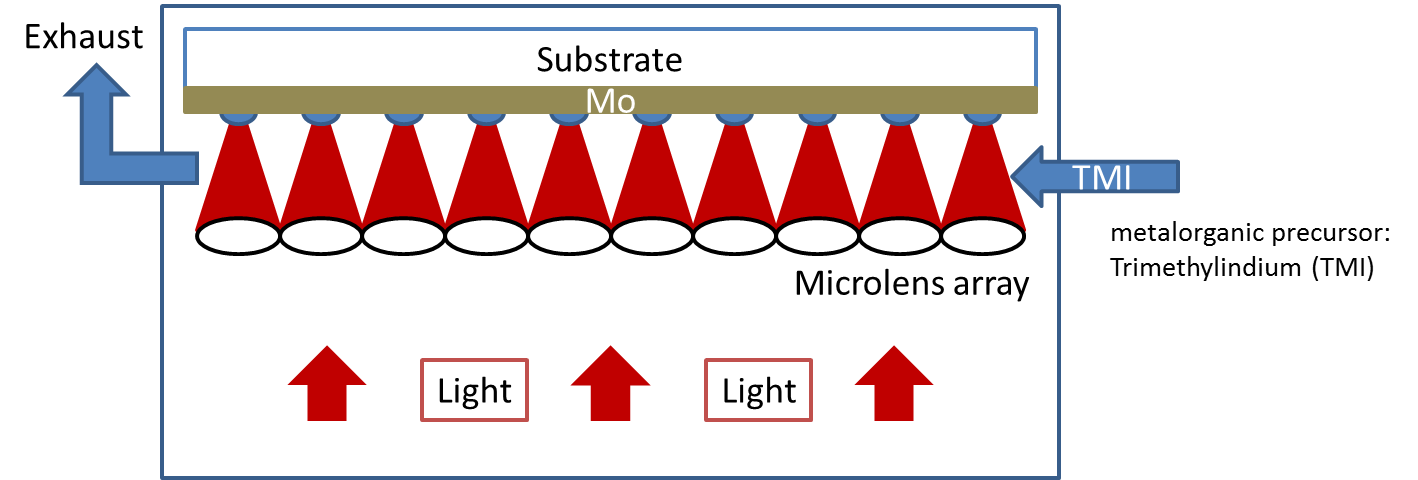
The objective is the realization of localized structure formation on amorphous surfaces without the application of complex and expensive mask or lithography processes. For this purpose, focused laser radiation of suitable wavelength and intensity is to be used, which is guided over the surface by a scanner in a grid-like manner, so that a pattern-shaped energy input can be made possible. The resulting thermal inhomogeneity is intended to cause the selective formation of liquid and ultimately crystalline structures on the surface.
Such islands can serve as precursors for the locally defined growth of compound semiconductors. The ministry of economics is funding the project with 1.5 million euros, of which around 700T euros will be allocated to the IKZ.
More Information:
Torsten Boeck
Section Semiconductor Nanostructures


