IKZ is the only EU research institute which offers 2” Aluminum Nitride (AlN) and Gallium Oxide (Ga₂O₃) crystal substrates to selected technology partners for developing disruptive power electronics technologies. To strengthen this mission, IKZ invested several million € in 2025 to extend its hardware platform to achieve this goal by early 2026.
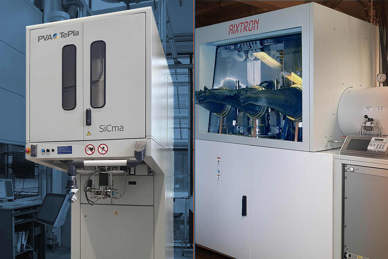
IKZ installed together with the industry company PVA Tepla a physical vapor transport growth reactor to grow AlN crystals in the range from 2” to 4” in the coming years. A further project partner is the industry company Siltronic.
In addition, within the framework of the EFRE project G.O.A.L (EFRE 1.6-14), an AIXTRON MOCVD epitaxy reactor with a 3x2-inch to 1x4-inch capacity was installed through investment funding, in order to realize the scaling of high-quality Ga₂O₃ epitaxial layers with outstanding homogeneity and thickness. With this, IKZ aims to establish itself as Europe-wide research partner and supplier of Ga₂O₃ epi-wafers as a base material for power electronics devices.
Without doubt, IKZ´EU flagship role to provide disruptive crystal materials on a prototyping scale will be strengthened by these invests.
Contact:
Leibniz-Institut für Kristallzüchtung (IKZ)
Dr. Carsten Hartmann
Group leader Aluminum Nitride Prototyping
Phone: +49 (30) 246 499 602
Email: carsten.hartmannikz-berlin.de
Dr. Andreas Popp
Group leader Epitaxy of semiconducting Gallium Oxide
Phone: +49 (30) 246 499 312
Email: andreas.poppikz-berlin.de